Film forming method for semiconductor device

a technology of semiconductor devices and film forming methods, which is applied in the direction of coatings, metallic material coating processes, chemical vapor deposition coatings, etc., can solve the problems of metal remains, conventional dielectric film formation methods, and cannot be removed by dry etching, so as to achieve great controllability and high credibility

Active Publication Date: 2007-07-10
PANASONIC CORP
View PDF12 Cites 0 Cited by
  • Summary
  • Abstract
  • Description
  • Claims
  • Application Information

AI Technical Summary

Benefits of technology

[0010]Considering the above mentioned problems, the present invention provides a film forming method for a semiconductor apparatus which has high credibility at the time of manufacturing and also has a great controllability.
[0013]Thus, the present invention can prevent the roughness on the surface of the silicon oxide film moderately and control the resistance value of the thin film resistance by making the thickness of the second silicon oxide film using low concentration.
[0014]As above explained, the film forming method of the semiconductor device according to the present invention has good step coverage and can control the roughness of the surface of the ozone TEOS film. Therefore, the credibility of the semiconductor device becomes higher, preventing moisture to enter.

Problems solved by technology

However, in the case where elements such as FET and HBT are previously formed, the metal remains around a step unit of the element and cannot be removed by dry etching.
However, the conventional dielectric film formation method has a following problem.
However, if the ozone TEOS film is formed using ozone with high concentration to moderate the step, the surface of the ozone TEOS film becomes rougher.
As the result, the resistance value of the thin film resistance on the ozone TEOS film changes so that a designed resistance value cannot be obtained.

Method used


Image

  • Film forming method for semiconductor device
  • Film forming method for semiconductor device
  • Film forming method for semiconductor device

Examples


Embodiment Construction

)

[0023]The film forming method for the semiconductor device according to the embodiment of the present invention is explained with reference to figures. Note that, numeric values used in the following explanation are examples.

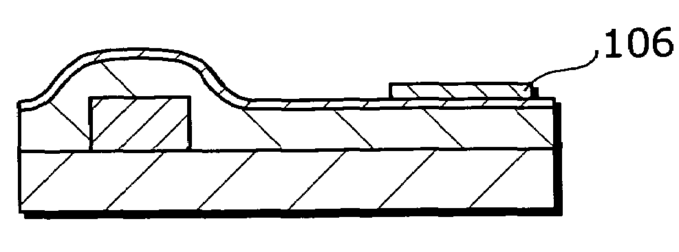
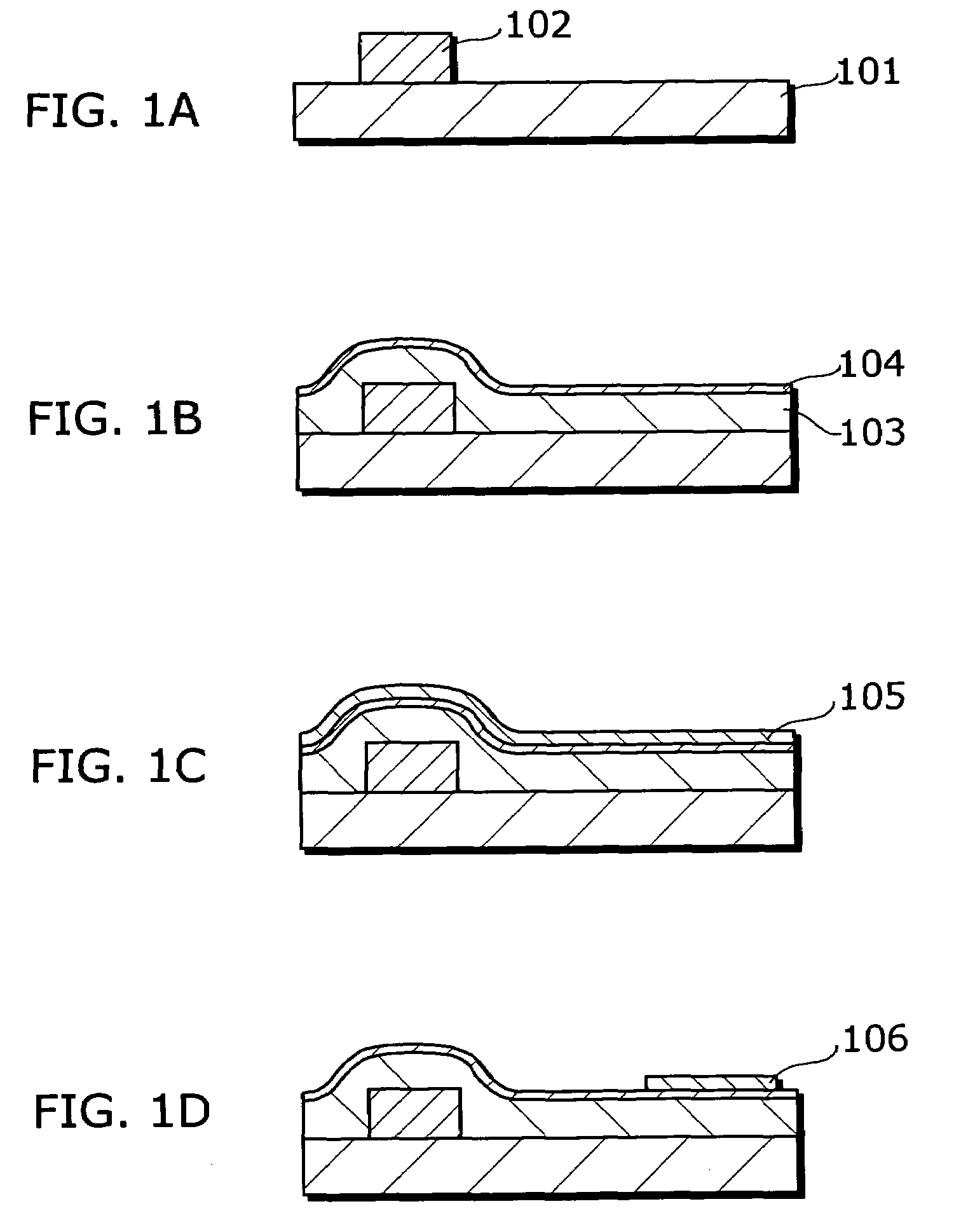
[0024]FIGS. 1A, 1B, 1C and 1D are process cross-section diagrams of the semiconductor device according to the embodiment of the present invention. First, as shown in FIG. 1A, a step unit 102 with about 1 μm height is formed by forming elements such as HBT on a semiconductor substrate 101 which made up with semi-insulating GaAs. Note that, the step unit 102 is an electrode and the like.

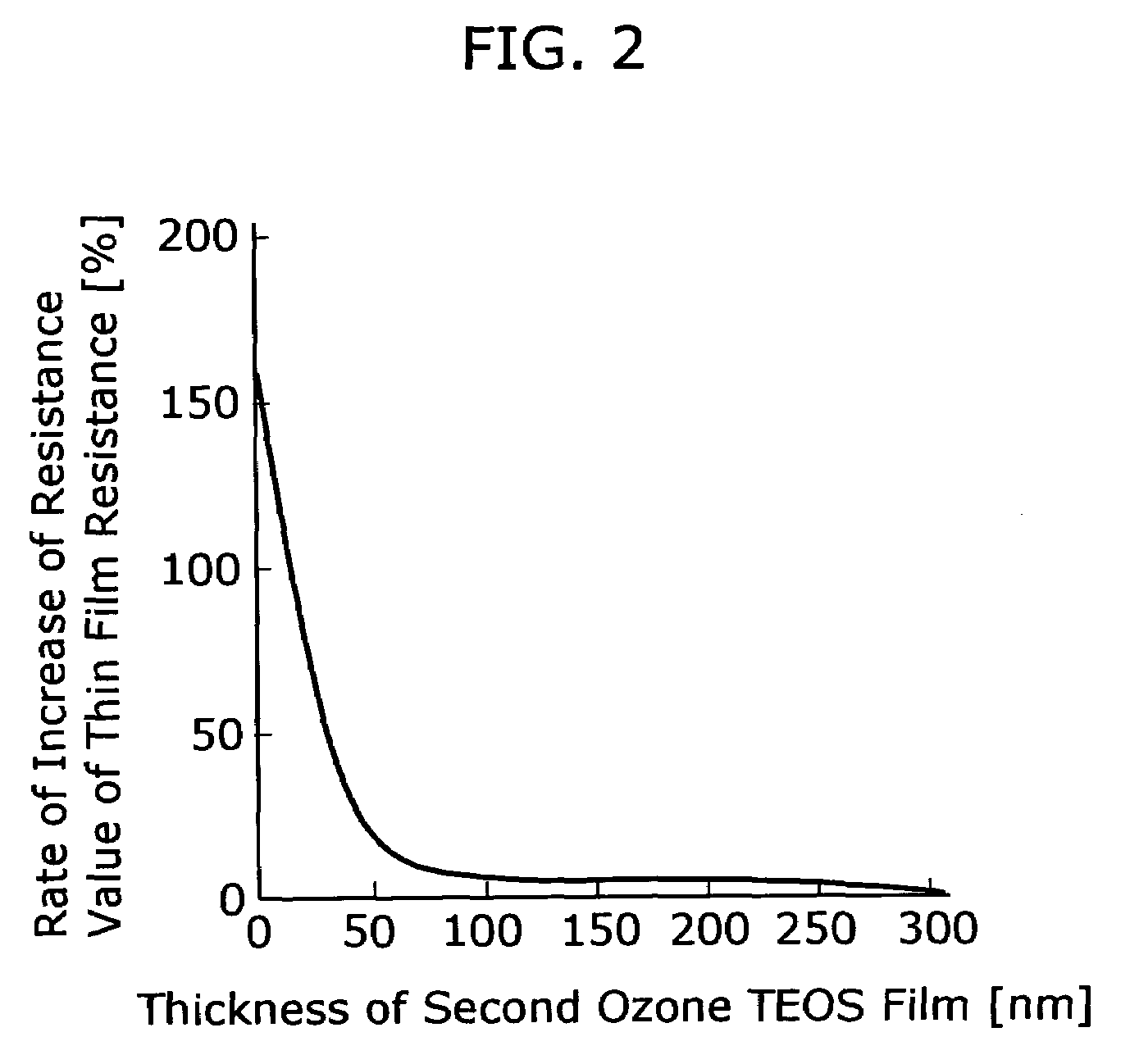
[0025]Next, as shown in FIG. 1B, the first ozone TEOS film 103 with the thickness of 900 nm is formed by the normal pressure CVD method that uses mixed gas of tetraethoxysilane with ozone. The temperature of the substrate at this time is 350° C. and the ozone concentration is 140 g / m3. Then, the second ozone TEOS film 104 with the thickness of 100 nm is formed by reducing the ozon...


PUM

PropertyMeasurementUnit
thicknessaaaaaaaaaa
concentrationaaaaaaaaaa
thicknessaaaaaaaaaa

Abstract

A method of forming films in a semiconductor device that can appropriately control a resistance value of a thin film resistance on an ozone TEOS film while preventing a metal thin film from remaining around a surface step unit after the metal thin film was dry etched. First, as shown in FIG. 1A, a step unit with the height of about 1 μm is formed by forming elements such as HBT on a semiconductor substrate made up of semi-insulating GaAs. Next, as shown in FIG. 1B, a first ozone TEOS film with the thickness of 900 nm by a Normal pressure CVD method using mixed gas of tetraethoxysilane with ozone. Then, a second ozone TEOS film with the thickness of 100 nm is formed by reducing the ozone concentration to 10 g / m3, while maintaining the substrate temperature at 350° C.

Description

BACKGROUND OF THE INVENTION[0001](1) Field of the Invention[0002]The present invention relates to a film forming method for a semiconductor device, and in particular to a method of forming interlayer dielectric films on a semiconductor device which has step units.[0003](2) Description of the Related Art[0004]A monolithic microwave integrated circuit (MMIC) which is a semiconductor integrated circuit designed for high frequency is formed by integrating active elements such as a field effect transistor (FET) and a hetero-junction bipolar transistor (HBT) into passive elements such as a resistance, an inductor and a capacitor on a single semiconductor substrate. Comparing to a single element, the MMIC can realize a reduction of a price because it can miniaturize and lighten microwave components. Furthermore, there is no need to connect between elements with a golden wire in the MMIC so that the high frequency characteristic is improved.[0005]A thin film resistance by metal such as tung...

Claims


Application Information

Patent Timeline
Patent Type & Authority Patents(United States)
IPC IPC(8): H01L21/31C23C16/40C23C16/44C23C16/455H01L21/316H01L21/768
CPCC23C16/402C23C16/45523H01L21/02164H01L21/02271H01L21/31612H01L21/76834H01L21/76837
Inventor HIKITA, MASAHIROUEMOTO, YASUHIRO
Owner PANASONIC CORP
Why Eureka
Try Eureka