Unlock instant, AI-driven research and patent intelligence for your innovation.

Semiconductor crystal based radiation detector and method of producing the same

a technology of semiconductors and radiation detectors, applied in the field of semiconductor crystal based radiation detectors, can solve the problems of reducing the resolution ability of radiation detectors, limited performance of radiation detectors,

Active Publication Date: 2012-11-20
GENERAL ELECTRIC CO
View PDF8 Cites 8 Cited by
  • Summary
  • Abstract
  • Description
  • Claims
  • Application Information

AI Technical Summary

Benefits of technology

The solution significantly reduces leakage currents and improves energy resolution, allowing for better detection of ionizing radiation by creating a controlled electrical environment that enhances signal collection and reduces noise.

Problems solved by technology

However, performance of the radiation detectors is typically limited by leakage currents which reduce the ability of the radiation detector to resolve the ionizing radiation.

Method used


Image

  • Semiconductor crystal based radiation detector and method of producing the same
  • Semiconductor crystal based radiation detector and method of producing the same
  • Semiconductor crystal based radiation detector and method of producing the same

Examples


Embodiment Construction

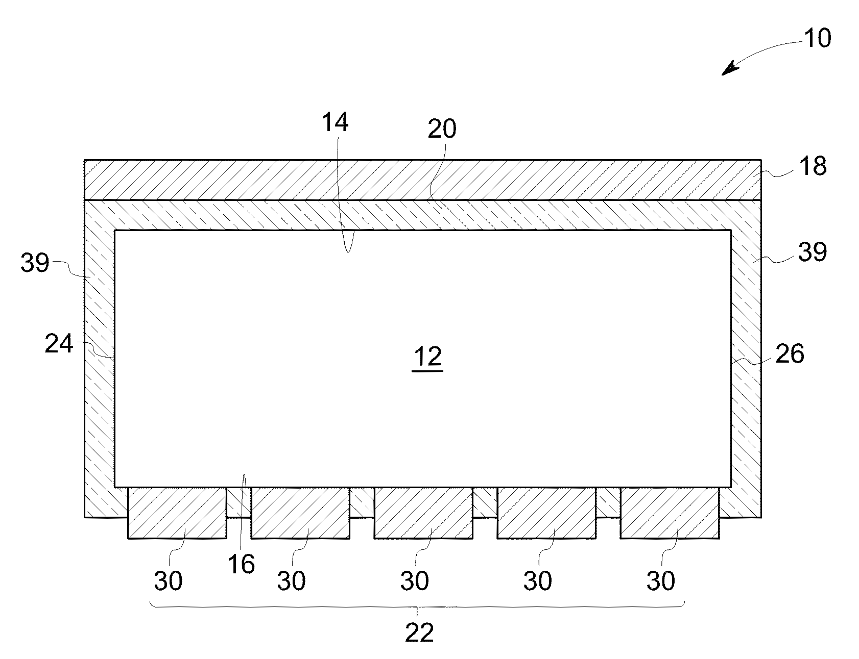
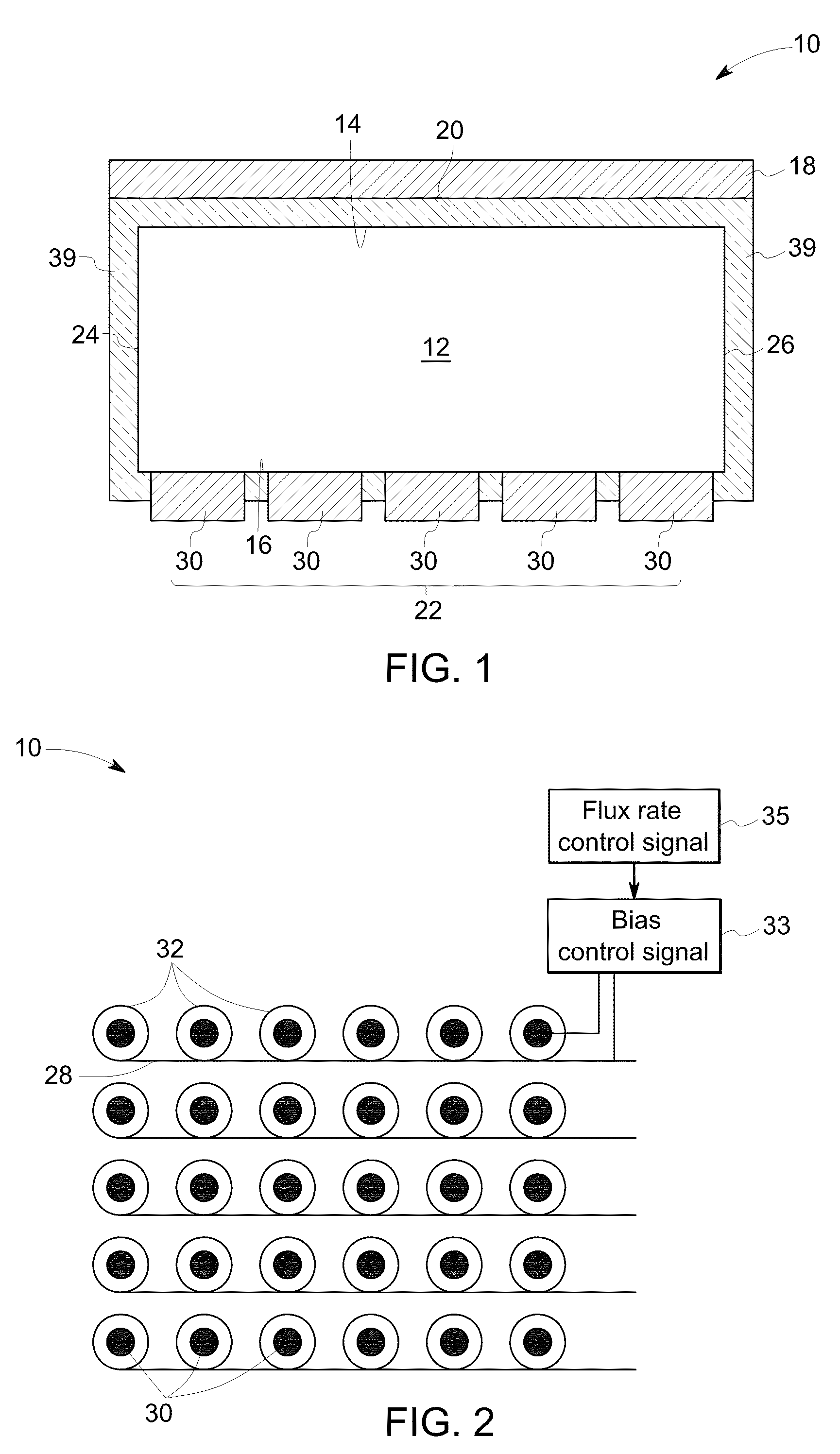
[0018]Embodiments disclosed herein relate to a semiconductor crystal based radiation detector. The radiation detector comprises an insulating layer between a semiconductor crystal and an electrode, for reducing leakage current of the radiation detector. Embodiments disclosed herein related to a method of producing a radiation detector. The method comprises an etching process to form a gradient tellurium-rich layer on a semiconductor crystal block. Embodiments of the invention are discussed below with reference to the drawing figures. For purposes of simplicity of description, common elements across different embodiments share the same reference numbers.

[0019]Referring to FIG. 1, an exemplary radiation detector 10 comprises a semiconductor crystal 12 having a first surface 14 and a second surface 16 opposite to the first surface 14. A first electrode 18 is electrically coupled with one of the first and second surfaces 14, 16 of the semiconductor crystal 12 to allow current to flow be...


PUM


Abstract

A radiation detector includes a semiconductor crystal having a first surface and a second surface opposite to the first surface, a first electrode electrically coupled with the first surface of the semiconductor crystal to allow current to flow between the first electrode and the crystal, and an insulating layer on the first surface and between the semiconductor crystal and the first electrode so as to create a partially transmissive electrical barrier between the first electrode and the crystal. The insulating layer has a thickness ranging from about 50 nanometers to about 500 nanometers.

Description

BACKGROUND[0001]Embodiments of the invention are generally related to the field of radiation detectors, and more particularly, to a semiconductor crystal based radiation detector and a method of producing the detector.[0002]Semiconductor crystal based radiation detectors are used for detecting ionizing radiation due to their ability to operate at room temperature, their small size and durability, and other features inherent in semiconductor crystals. Such detectors are used in a wide variety of applications, including medical diagnostic imaging, nuclear waste monitoring, industrial process monitoring, and space astronomy. Ionizing radiation includes both particulate radiation, such as alpha or beta particles, and electromagnetic radiation such as gamma or X-rays.[0003]The semiconductor crystal based radiation detectors generally employ semiconductor materials, such as Cd—Zn—Te (CZT) which has a wide band-gap. A conventional CZT radiation detector typically comprises a CZT crystal lo...

Claims


Application Information

Patent Timeline
Patent Type & Authority Patents(United States)
IPC IPC(8): G01T1/24
CPCH01L31/115H01L31/1185
Inventor ZHANG, MINGLONGDU, YANFENGTKACZYK, JOHN ERICWU, ZHAOPINGBLEVIS, IRA
Owner GENERAL ELECTRIC CO