Apparatus and method for preventing charge pumping in series connected diode stacks

a series connected diode and charge pumping technology, applied in the field of light sensor circuits, can solve the problems of affecting the operation of ambient light sensors, affecting the accuracy of voltage control, and difficult to achieve precision voltage control in practice, so as to reduce forward bias voltage and suppress charge pumping

Active Publication Date: 2012-12-11
SHARP KK
View PDF11 Cites 0 Cited by
  • Summary
  • Abstract
  • Description
  • Claims
  • Application Information

AI Technical Summary

Benefits of technology

[0026]The apparatus and method in accordance with the present invention are able to suppress charge pumping without requiring adoption of an alternative display architecture, where the counter-electrode voltage remains static.

Problems solved by technology

If an electric field of non-zero mean is maintained over the LC material, it will suffer degradation.
The current which flows on account of a non-zero bias voltage is detrimental to the operation of an ambient light sensor, as it cannot be distinguished from that which flows due to incident illumination.
However, such precision voltage control can be difficult to achieve in practice.
However, series connected diodes have a disadvantage when employed within an electrically noisy environment.
Unfortunately, the asymmetric conduction characteristic of the diode, shown in FIG. 5, may cause a net forward current to flow in the presence of electrical interference.
This net current is indistinguishable from that which arises due to illumination, and therefore corrupts the ambient light measurement.
Such uneven voltage perturbations may increase the transient forward bias voltages across diodes within the stack, raising the charge pumping current.
Nonetheless, it may not be possible to reduce the shield resistance to zero and hence the voltage perturbations sufficiently, and so the residual charge pumping current may still be unacceptable.
However, higher absolute voltages must be generated on the TFT glass 30 of such displays, increasing complexity of the drive circuits.

Method used


Image

  • Apparatus and method for preventing charge pumping in series connected diode stacks
  • Apparatus and method for preventing charge pumping in series connected diode stacks
  • Apparatus and method for preventing charge pumping in series connected diode stacks

Examples


first embodiment

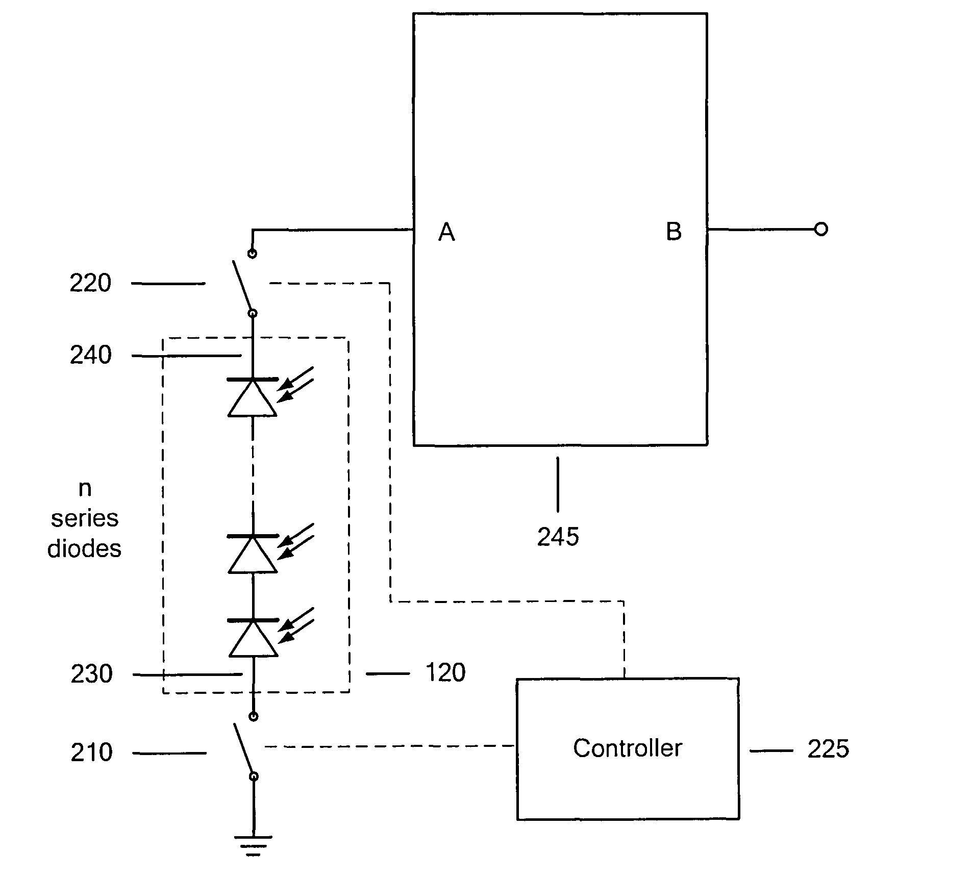
[0078]A device in accordance with the invention is shown in FIGS. 12 and 13, and finds use in situations where no conductive shield layer is present above the diode stack. FIG. 12 is a schematic diagram showing a stack 120 of at least two series connected photodiodes, arranged such that the cathode of one is connected to the anode of the next. The end-most anode 230 is connected to one terminal of a simple two terminal switch 210, the other terminal of this switch being connected to ground. The end-most cathode 240 is connected to one terminal of a second two terminal switch 220, the other end of this switch being connected to terminal ‘A’ of bias and current measurement circuitry 245. This bias generating and current measurement circuitry 245 is embodied in the form of an integrator 70 as shown in FIG. 3, and described in WO2008 / 044749A1. The switches 210 and 220 are controlled via a controller 225, which commands the switches to open and close using known techniques. Although not ...

second embodiment

[0080]FIGS. 12 and 15 show a device in accordance with the invention, whereby the switches 210 and 220 are operated as shown in FIG. 15. The switches close only when the counter-electrode voltage is static, as was shown in FIG. 13. However, in FIG. 15 the switches close once every second low pulse or once every second high pulse of the counter-electrode waveform, rather than once every period. This may be advantageous, as it reduces the rate at which the switches are being operated and hence reduces the frequency of noise which couples from the switch signals themselves to other parts of the circuitry (such as to the bias generation and current measurement circuitry 245).

third embodiment

[0081]FIGS. 12 and 16 show a device in accordance with a third and preferred embodiment of the invention, whereby switches 210 and 220 are operated in the manner shown in FIG. 16. The third embodiment is used when a shield layer 180 is present above the diode stack 120. FIG. 16 shows that the switches are closed following each transition of the counter-electrode voltage and once the voltage upon the conductive shield layer has settled. A short delay is utilized between each transition ending and the switches being closed, allowing time for transient voltages within the diode stack to decay to levels which will not produce a significant charge pumping current. On each occasion the switches are opened before a new transition of the counter-electrode voltage occurs, as this will be accompanied by transient voltages within the stack. This embodiment is preferred because the switches may be opened more frequently than other embodiments. This is beneficial when the diode stack current mus...


PUM


Abstract

An ambient light sensor includes a first stack of at least two photodiodes, wherein a cathode of one of the at least two photodiodes is electrically connected to an anode of another of the at least two photodiodes. The ALS further includes a bias source for providing a bias voltage to the first stack, and at least one switch electrically connected to the first stack. The at least one switch is operative to periodically apply the bias voltage to and remove the bias voltage from the first diode stack.

Description

RELATED APPLICATION DATA[0001]This application claims priority of U.S. Provisional Application No. 61 / 261,880 filed on Nov. 17, 2009, which is incorporated herein by reference in its entirety.TECHNICAL FIELD[0002]The present invention relates to light sensor circuits and, more particularly, to an apparatus and method for reducing average noise currents in series connected diode stacks of light sensor circuits used in display systems.BACKGROUND OF THE INVENTION[0003]FIG. 1 shows a simplified cross-section of a typical transmissive active-matrix liquid crystal display (AMLCD). The backlight 10 serves as a light source for illumination of the display. The transmission of light through the display, from the backlight 10 to the viewer 20, is controlled by the use of electronic circuits made from thin film transistors (TFTs). These TFTs are fabricated on a glass substrate (known as the TFT glass 30) and are operated in conjunction with a ‘counter-electrode’40 so as to vary the local elect...

Claims


Application Information

Patent Timeline
Patent Type & Authority Patents(United States)
IPC IPC(8): G01J1/44
CPCG01J1/32G01J1/44G01J1/4204
Inventor COULSON, MICHAEL P.WASHIO, HAJIMEHADWEN, BENJAMIN J.SHAH, SUNAY
Owner SHARP KK
Why Eureka
Try Eureka