Multi-plane type flash memory and methods of controlling program and read operations thereof

a program technology, applied in the field of flash memory devices, can solve the problems of cumbersome requirements, longer whole program time of multi-plane type flash memory devices, and cumbersome requirements, and achieve the effect of improving operation speed and data throughpu

Active Publication Date: 2013-01-01
SK HYNIX INC
View PDF23 Cites 86 Cited by
  • Summary
  • Abstract
  • Description
  • Claims
  • Application Information

AI Technical Summary

Benefits of technology

This patent relates to improving the operation speed and data throughput of flash memory devices by simultaneously conducting program and read operations for multiple planes in response to a chip enable signal containing multiple bits, without needing to build complicated circuits. The method allows for faster processing and higher data throughput.

Problems solved by technology

Therefore, it needs to repeat the aforementioned procedure in order to complete the program operation for all of the memory cell blocks B1˜BK, which causes the whole program time to be longer due to an increase of the number of the memory cell blocks.
Therefore, there is a problem that the whole program time of the multi-plane type flash memory device is longer than the whole program time of the single-plane flash memory device.
Furthermore, there is the cumbersome that it is required of selecting one of the planes and generating an address signal by an external memory controller in addition to a block address in order to program data in the selected plane or to read data from the selected plane.
And, the flash memory device needs to comprise complicated control circuits to regulate the planes each by each.

Method used


Image

  • Multi-plane type flash memory and methods of controlling program and read operations thereof
  • Multi-plane type flash memory and methods of controlling program and read operations thereof
  • Multi-plane type flash memory and methods of controlling program and read operations thereof

Examples


Embodiment Construction

[0019]Preferred embodiments of the present invention will be described below in more detail with reference to the accompanying drawings. The present invention may, however, be embodied in different forms and should not be constructed as limited to the embodiments set forth herein. Rather, these embodiments are provided so that this disclosure will be thorough and complete, and will fully convey the scope of the invention to those skilled in the art. Like numerals refer to like elements throughout the specification.

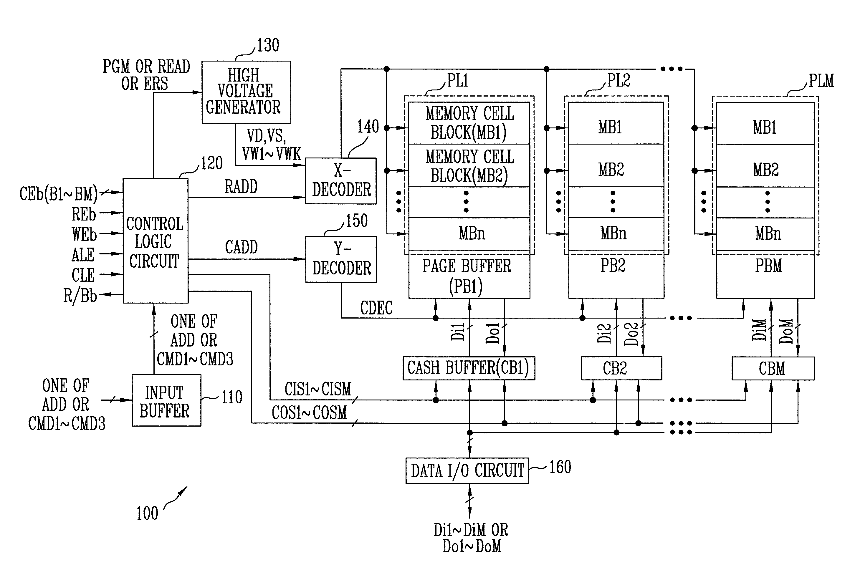
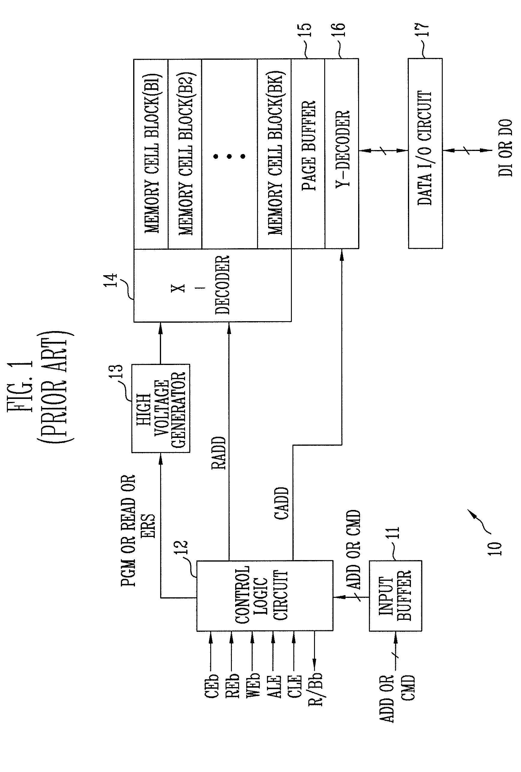
[0020]FIG. 3 is a block diagram of a conventional flash memory device. Referring to FIG. 3, the flash memory device 100 is comprised of an input buffer 110, a control logic circuit 120, a high voltage generator 130, an X-decoder 140, a plurality of planes PL1˜PLM (M is an integer), a plurality of page buffers PB1˜PBM (M is an integer), a plurality of cache buffers CB1˜CBM (M is an integer), and a data input / output circuit 160. The input buffer 110 receives and an external ...


PUM


Abstract

A multi-plane type flash memory device comprises a plurality of planes each including a plurality of memory cell blocks, page buffers each latching an input data bit to be output to its corresponding plane or latching an output data bit to be received from the corresponding plane, cache buffers each storing an input or output data bits in response to one of cache input control signals and each transferring the stored data bit to the page buffer or an external device in response to one of cache output control signals, and a control logic circuit generating the cache input and output control signals in response to command and chip enable signals containing plural bits. The program and read operations for the plural planes are conducted simultaneously in response to the chip enable signal containing the plural bits, which increases an operation speed and data throughput processed therein.

Description

CROSS-REFERENCES TO RELATED APPLICATIONS[0001]The present application is a continuation of U.S. patent application Ser. No. 11 / 159,542, filed Jun. 22, 2005, which claims priority to Korean Patent Application No. 10-2005-0020169, filed Mar. 10, 2005, both of which are incorporated by reference.BACKGROUND OF THE INVENTION[0002]The present invention relates to flash memory devices and specifically, to a multi-plane type flash memory device and method of controlling program and read operations thereof.[0003]Flash memory devices may be generally classified into single-plane types and multi-plane types in accordance with the structural configuration of memory cell array thereof. The single-plane type flash memory device includes a single plane composed of a plurality of memory cell blocks, while the multi-plane type flash memory device includes a plurality of planes each being composed of a plurality of memory cell blocks. FIG. 1 is a block diagram of a conventional flash memory device, s...

Claims


Application Information

Patent Timeline
Patent Type & Authority Patents(United States)
IPC IPC(8): G06F13/00G06F13/28G11C7/00G11C8/00G11C7/18
CPCG11C16/10G11C16/26B01D35/00B01D35/18C02F1/78B01D29/56B01D2201/16
Inventor YOU, BYOUNG SUNG
Owner SK HYNIX INC
Why Eureka
Try Eureka