Apparatus for manufacturing group III nitride semiconductor

Active Publication Date: 2013-01-08
TOYODA GOSEI CO LTD
View PDF7 Cites 0 Cited by
  • Summary
  • Abstract
  • Description
  • Claims
  • Application Information

AI Technical Summary

Benefits of technology

[0023]According to the apparatus for manufacturing a Group III nitride semiconductor of the present invention, since the glove box and the pressure vessel can maintain the same internal atmosphere, after weighing within the glove box, the reaction vessel can be disposed in the pressure vessel without involvement of oxidation of flux or a like problem. This eliminates the need to completely seal the reaction vessel and allows use of a large-sized reusable reaction

Problems solved by technology

In the case where a large-sized reaction vessel is used, since such a large-sized reaction vessel made of SUS is expensive, the reaction vessel is required to be reusable.
However, since such a reusable reaction vessel cannot be completely sealed, the method of Japanese Patent Application Laid-Open (kokai) No. 2003-286099 involves a drawbac

Method used


Image

  • Apparatus for manufacturing group III nitride semiconductor
  • Apparatus for manufacturing group III nitride semiconductor
  • Apparatus for manufacturing group III nitride semiconductor

Examples


Example

Embodiment 1

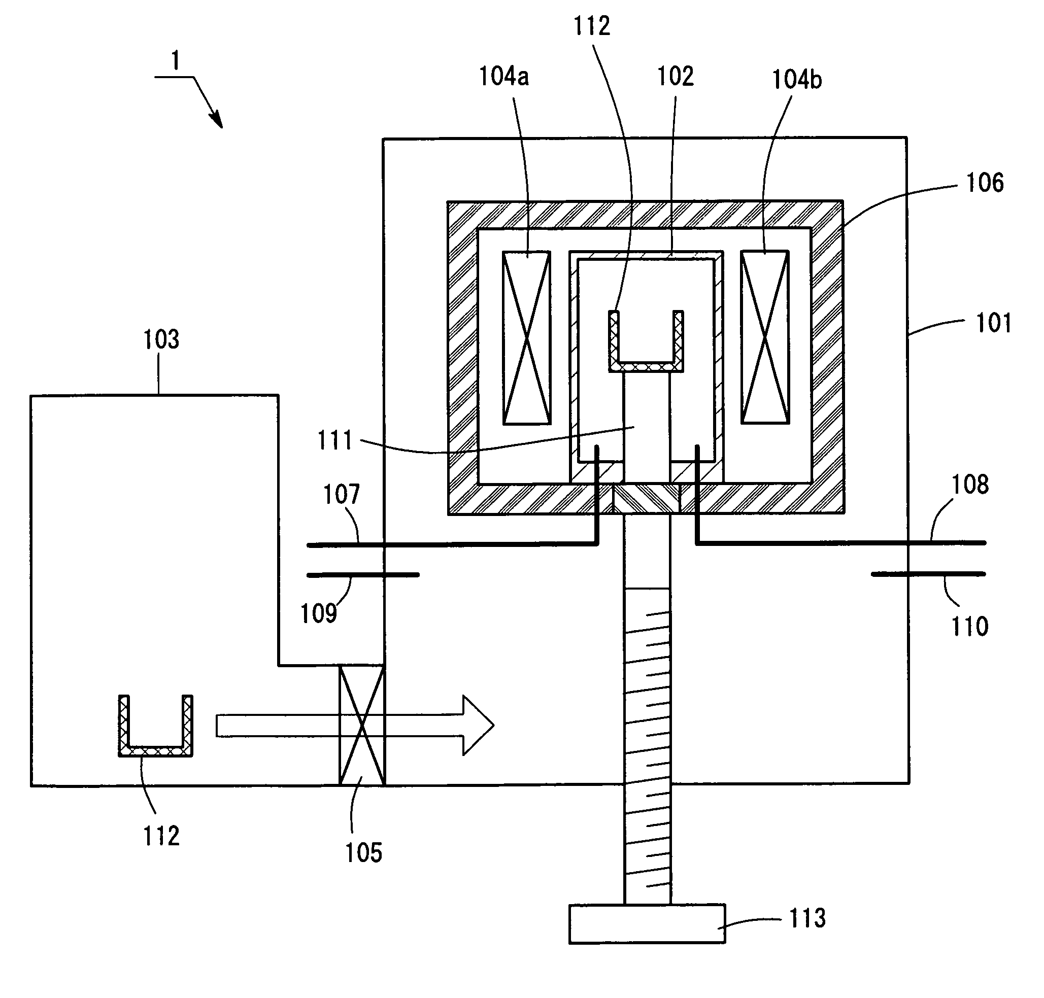
[0033]FIG. 1 schematically shows the configuration of a Group-III-nitride-semiconductor manufacturing apparatus 1 according to Embodiment 1 of the present invention. The Group-III-nitride-semiconductor manufacturing apparatus 1 is used to manufacture a Group III nitride semiconductor according to a flux method. The configuration of the Group-III-nitride-semiconductor manufacturing apparatus 1 is described below.

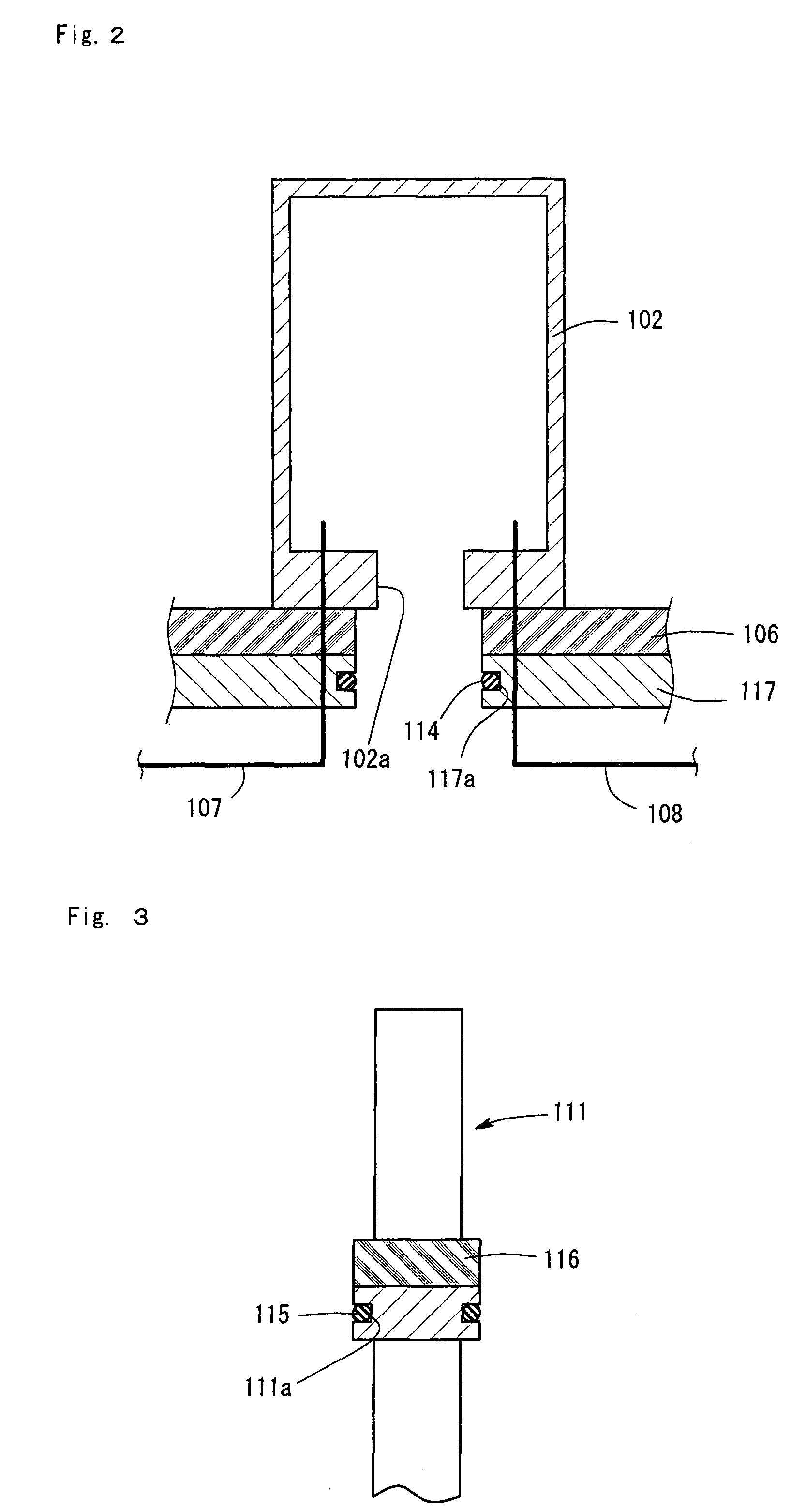
[0034]The Group-III-nitride-semiconductor manufacturing apparatus 1 includes a pressure vessel 101; a reaction vessel 102 disposed within the pressure vessel 101; heating devices 104a and 104b disposed within the pressure vessel 101 and adapted to heat the reaction vessel 102; and a glove box 103 filled with argon gas. The pressure vessel 101 and the glove box 103 are connected to each other via a gate valve 105 which can be opened and closed. When the gate valve 105 is opened, the pressure vessel 101 and the glove box 103 can have the same internal atmosphere. Th...

Example

Embodiment 2

[0046]FIG. 5 schematically shows the configuration of a Group-III-nitride-semiconductor manufacturing apparatus 2 according to Embodiment 2 of the present invention. The configuration of the apparatus 2 is described below.

[0047]The Group-III-nitride-semiconductor manufacturing apparatus 2 includes a horizontal pressure vessel 201; a reaction vessel 202 to be disposed within the pressure vessel 201; heating devices 204a and 204b for heating the reaction vessel 202 to be disposed within the pressure vessel 201; and a glove box 203 filled with argon gas.

[0048]A flanged lid 201a can open and close an opening portion 221 of the pressure vessel 201. The pressure vessel 201 and the glove box 203 are connected horizontally to each other such that the opening portion 221 of the pressure vessel 201 is exposed to the interior of the glove box 203. The flanged lid 201a and the glove box 203 are connected to each other via bellows 222. A moving device 220 is connected to the flanged ...

Example

Embodiment 3

[0058]FIG. 6 schematically shows the configuration of a Group-III-nitride-semiconductor manufacturing apparatus 3 according to Embodiment 3 of the present invention. The configuration of the apparatus 3 is described below.

[0059]The Group-III-nitride-semiconductor manufacturing apparatus 3 includes a horizontal pressure vessel 301; a reaction vessel 302 to be disposed within the pressure vessel 301; heating devices 304a and 304b for heating the reaction vessel 302 to be disposed within the pressure vessel 301; and a glove box 303 filled with argon gas.

[0060]A flanged lid 301a can open and close an opening portion 321 of the pressure vessel 301. Similar to Embodiment 2, the pressure vessel 301 and the glove box 303 are connected horizontally to each other such that the opening portion 321 of the pressure vessel 301 is exposed to the interior of the glove box 303. However, the pressure vessel 301 and the glove box 303 are connected to each other via bellows 322. By moving t...


PUM


Abstract

An apparatus for manufacturing a Group III nitride semiconductor is composed of a pressure vessel, a reaction vessel disposed within the pressure vessel, a heating device disposed within the pressure vessel so as to heat the reaction vessel, and a glove box filled with argon gas. The pressure vessel and the glove box are connected to each other via a gate valve. By virtue of this configuration, a large-sized reusable reaction vessel can be disposed within the pressure vessel without causing oxidation of Na.

Description

BACKGROUND OF THE INVENTION[0001]1. Field of the Invention[0002]The present invention relates to an apparatus for manufacturing a Group III nitride semiconductor, and particularly to an apparatus for manufacturing a Group III nitride semiconductor according to an Na flux method.[0003]2. Description of the Related Art[0004]Conventionally, an Na flux method for growing a Group III nitride semiconductor crystal is known. According to the Na flux method, sodium (Na) and gallium (Ga) are melted, and a resultant mixed melt is maintained at a temperature of about 800° C. The mixed melt is subjected to reaction with nitrogen under a high pressure of about 100 atmospheres, thereby growing a gallium nitride (GaN) crystal on the surface of a seed crystal.[0005]In order to yield GaN having a low impurity content by the Na flux method, high-purity Na is required. Since Na is highly reactive and highly susceptible to oxidization, weighing and like work are carried out within a glove box filled wi...

Claims


Application Information

Patent Timeline
IPC IPC(8): C30B35/00C30B11/00
CPCC01B21/0632C30B9/00C30B29/403Y10T117/10Y10T117/1024
Inventor YAMAZAKI, SHIROHIRATA, KOJI
Owner TOYODA GOSEI CO LTD
Why Eureka
Try Eureka