Liquid crystal display device with enhanced brightness

a liquid crystal display and brightness technology, applied in non-linear optics, instruments, optics, etc., can solve the problems of not necessarily achieving a sufficiently high aperture ratio, no improvement proposal in this regard, etc., to prevent the low liquid crystal controllability from contributing to the display, suppress the disturbance of the electric field, and reduce the effect of distortion

Active Publication Date: 2013-01-08
JAPAN DISPLAY WEST
View PDF7 Cites 3 Cited by
  • Summary
  • Abstract
  • Description
  • Claims
  • Application Information

AI Technical Summary

Benefits of technology

[0006]It is therefore desirable to provide a liquid crystal display device capable of increasing brightness by improving a structure for applying drive voltage to a pixel electrode.
[0009]In the liquid crystal display device according to an embodiment of the invention, preferably, the interlayer conductor has a first extending portion which extends along a plane of a layer between the opposite electrode and the selection line so as to cover an overlap region where the opposite electrode hole partly overlaps the selection line. In this case, a leak electric field from the selection line to the liquid crystal layer via the opposite electrode hole is blocked by a part of the interlayer conductor extending along the layer stack plane, and disturbance of the electric field is suppressed. Preferably, the interlayer conductor further has a second extending portion different from the first extending portion, a first inner edge region of the opposite electrode, which is a part of a whole inner edge region surrounding the opposite electrode hole, faces the overlap region, and a second inner edge region of the opposite electrode, which is different from the first inner edge region, overlaps the second extending portion of the interlayer conductor or the pixel electrode, or overlaps both of the second extending portion of the interlayer conductor and the pixel electrode. In the case where the second inner edge region of the opposite electrode is covered with the pixel electrode, disturbance of the electric field which may occur when the second inner edge region is not covered with the pixel electrode is suppressed. Alternatively, in the case where the part of the interlayer conductor overlaps the second inner edge region, a part where no opposite electrode exists (liquid crystal controllability is low) is covered with the part of the interlayer conductor. Accordingly, even if the electric field generated between the pixel electrode and the opposite electrode is disturbed, a part of the interlayer insulating film blocks light. As a result, the part of low liquid crystal controllability is prevented from contributing to display. Therefore, drop in the contrast is prevented.
[0010]In the liquid crystal display device according to the embodiment of the present invention, since the opposite electrode hole which allows the interlayer conductor to pass therethrough is located in a position so as to overlap the selection line, the area of the transmission region may be enlarged, and display brightness improves. In addition, since the opening in the pixel electrode may be enlarged to a position closer to the selection line as compared with the conventional technique, the opening area is increased, and display contrast improves. Moreover, by utilizing a part of the selection line as a gate part of the thin film transistor, the space for disposing the thin film transistor is reduced, so that the area of the light transmission region may be further enlarged by the amount of the reduced space, and the opening in the pixel electrode may be enlarged, thereby, in this regard as well, contributing to improvement of the display brightness and display contrast.

Problems solved by technology

As described above, since the conductive contact is necessary to connect the pixel electrode and the TFT and the space for disposing the conductive contact is necessary, a sufficiently high aperture ratio is not necessarily obtained.
There is, however, no proposal for improvement in this regard.

Method used


Image

  • Liquid crystal display device with enhanced brightness
  • Liquid crystal display device with enhanced brightness
  • Liquid crystal display device with enhanced brightness

Examples


first embodiment

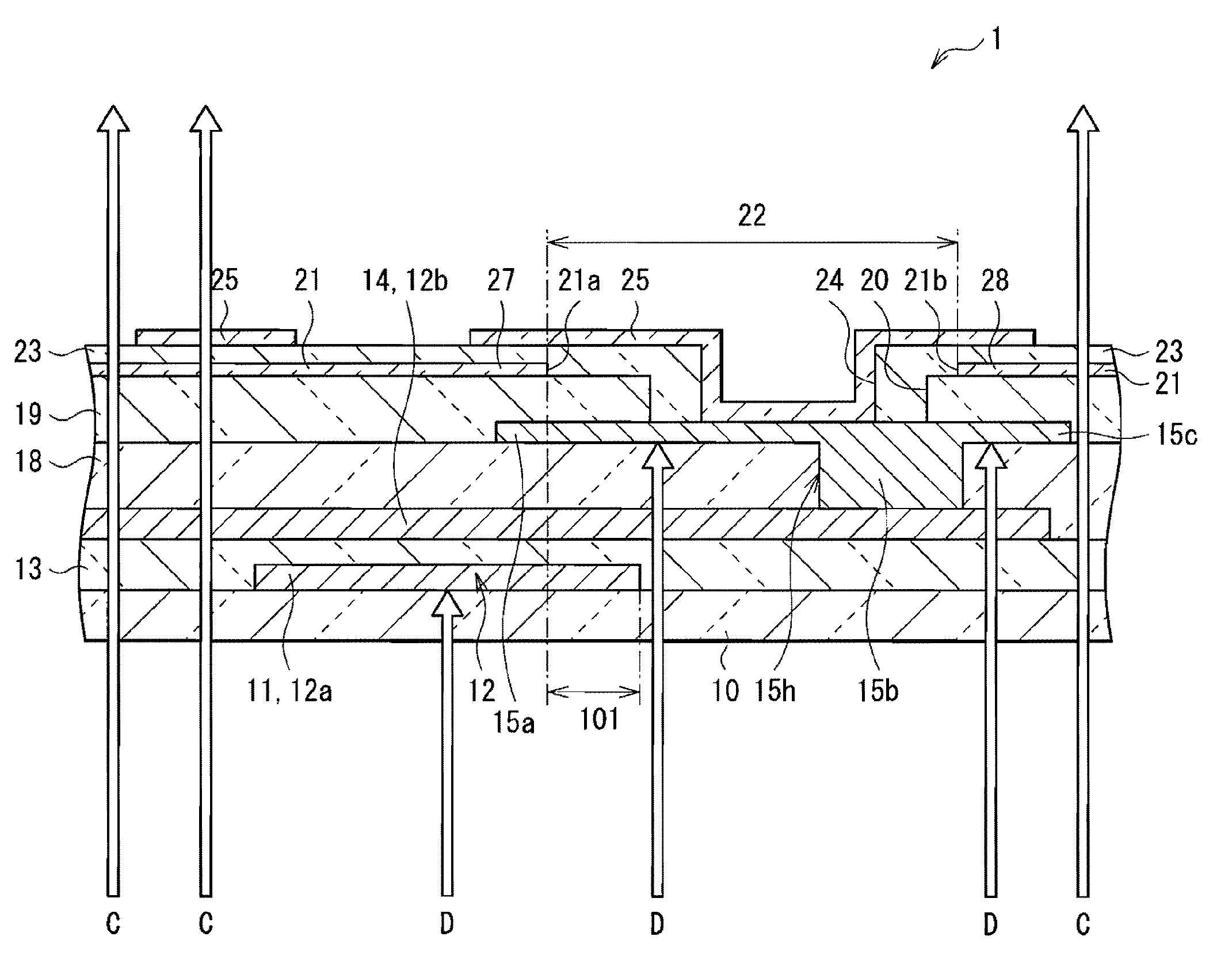
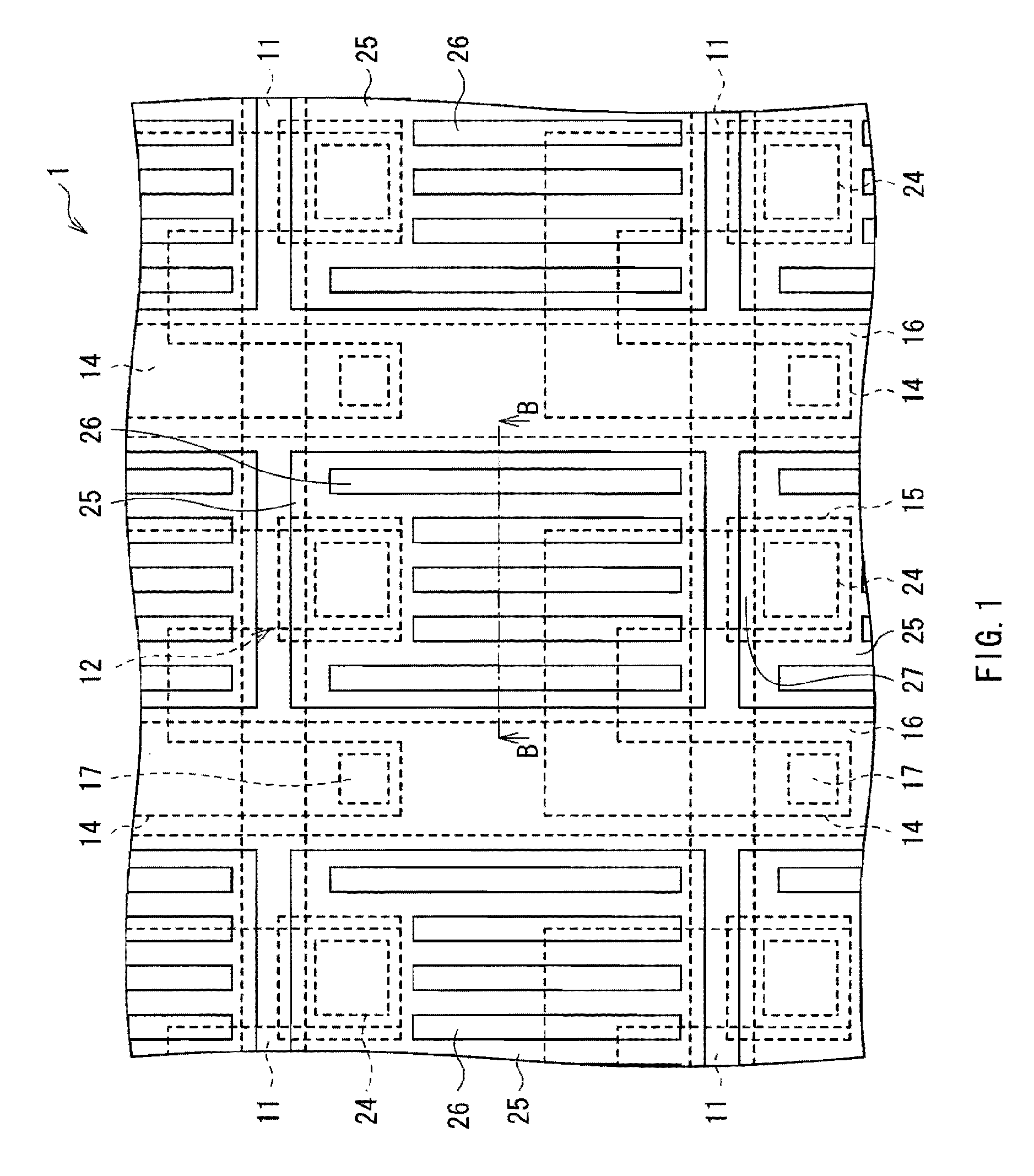
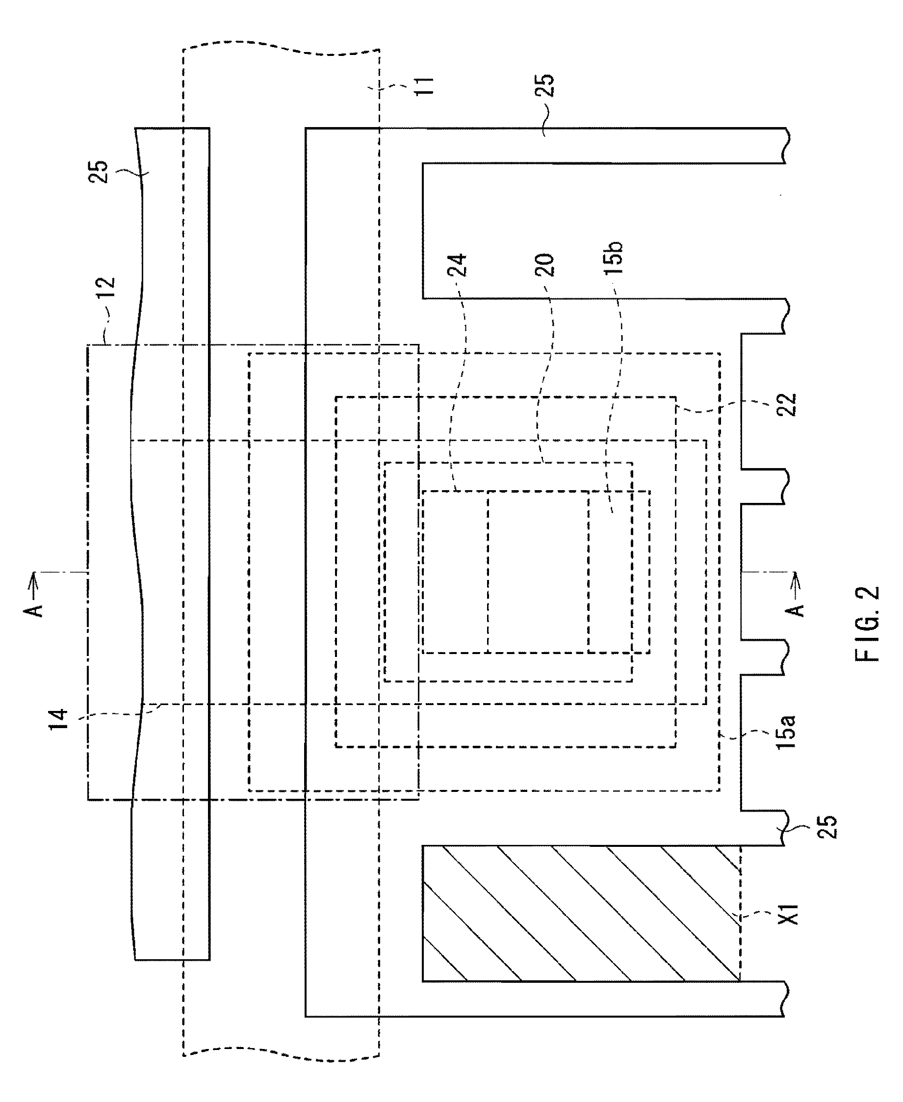
[0026]FIG. 1 is a plan view illustrating the configuration of a main part of a liquid crystal display device according to a first embodiment of the present invention. FIGS. 2 and 3 are enlarged views of a part (a part around a contact) in the liquid crystal display device illustrated in FIG. 1. In FIG. 3, a part of the components (such as a pixel electrode) is not illustrated. FIG. 4 illustrates a sectional structure taken along line A-A of FIG. 2.

[0027]As illustrated in FIG. 4, a liquid crystal display device 1 is provided with a glass substrate 10. On the top face of the glass substrate 10, a plurality of gate lines 11 as selection lines extend in the row direction (the direction perpendicular to the drawing surface). In a region of one pixel, the gate line 11 serves as a gate 12a of a switching element for driving the pixel, i.e., a thin film transistor (TFT) 12. On the top face of the glass substrate 10, a gate insulating film 13 is provided, and the gate lines 11 are covered wi...

second embodiment

[0068]FIG. 9 is an enlarged view of a portion of the first contact 15 in a liquid crystal display device 2 according to a second embodiment. The same reference numerals are designated to components similar to those of the first embodiment, and their description will not be repeated or will be given briefly. In the liquid crystal display device 2 of the second embodiment, two more slits 41 (the second slit from the right side and the second slit from the left side) out of slits 41 formed in the pixel electrode 40 are longer than those of the first embodiment, and a part of the slits 41 overlaps the extension part 15a of the first contact 15. In the second embodiment, four slits out of the slits 26 extend close to the gate 12a of the TFT 12. Therefore, as compared with the liquid crystal display device 1 of the first embodiment, a hatched region X2 in FIG. 9 becomes an incident light transmittable region, and display brightness improves by the amount of the region.

third embodiment

[0069]FIG. 10 is an enlarged view of a portion of the first contact 15 in a liquid crystal display device 3 according to a third embodiment. The liquid crystal display device 3 of the third embodiment is configured so that at least one of a side face in which the interlayer insulating film hole 20 is formed and a side face in which the pixel insulating film hole 24 is formed is in the same plane, and the slits 41 formed in the pixel electrode 40 are formed in a manner similar to those of the second embodiment illustrated in FIG. 9.

[0070]When all of side faces of the interlayer insulating film hole 20 and the pixel insulating film hole 24 are formed in the same plane, that is, the plane size of the interlayer insulating film hole 20 and that of the pixel insulating film hole 24 are set to the same and the holes 20 and 24 are disposed in the same position, the holes 20 and 24 may be formed by single etching. A concrete example of the process is as follows. On the top face of the trans...


PUM

PropertyMeasurementUnit
constant diameteraaaaaaaaaa
liquid crystal structureaaaaaaaaaa
insulatingaaaaaaaaaa

Abstract

A liquid crystal display device with enhanced brightness through improving a partial structure for applying potential to a pixel electrode is provided. The liquid crystal display device includes: a pixel electrode with a plurality of openings; an opposite electrode disposed to face the pixel electrode with an insulating layer in between; a liquid crystal layer disposed on an opposite side of the pixel electrode from the opposite electrode; a selection line utilized to select a pixel; a thin film transistor disposed on the opposite side of the opposite electrode from the pixel electrode as to drive the pixel and utilizing a part of the selection line as a gate thereof; and an interlayer conductor connecting between the thin film transistor and the pixel electrode. The opposite electrode has an opposite electrode hole which allows the interlayer conductor to pass therethrough, and the opposite electrode hole partly overlaps the selection line.

Description

BACKGROUND OF THE INVENTION[0001]1. Field of the Invention[0002]The present invention relates to a liquid crystal display device in which displaying is performed by a liquid crystal in an in-plane switching mode.[0003]2. Description of the Related Art[0004]There is a liquid crystal display device having a liquid crystal structure of an in-plane switching mode such as an FFS (Fringe Field Switching) mode. The liquid crystal display device in the FFS mode has an opposite electrode. A pixel electrode having a slit-shaped opening is disposed to oppose the opposite electrode through an insulating layer. Further, a liquid crystal layer is disposed above the pixel electrode. A conductive contact is disposed to penetrate the insulating layer in the layer stack direction, and the pixel electrode and a TFT (Thin Film Transistor) for driving the pixel electrode are made conductive via the conductive contact. In such a liquid crystal display device, when voltage is applied from a data line conn...

Claims


Application Information

Patent Timeline
Patent Type & Authority Patents(United States)
IPC IPC(8): G02F1/1343G02F1/136
CPCG02F1/134363G02F1/136227G02F2201/40G02F1/136G02F1/1343
Inventor KANAYA, YASUHIRONAKAJIMA, DAIKIYAGI, KEIICHI
Owner JAPAN DISPLAY WEST
Why Eureka
Try Eureka