Multispectral imaging device and manufacturing thereof

Active Publication Date: 2013-01-22
BANPIL PHOTONICS
View PDF10 Cites 42 Cited by
  • Summary
  • Abstract
  • Description
  • Claims
  • Application Information

AI Technical Summary

Benefits of technology

[0055]The invention offers to detect broad detection ranges varying from UV to mid infrared as high as 5500 nm with high quantum efficiency, high frequency response, and low signal-to-noise ratio. With proper design and fabrication process, N×N photodiodes array can be fabricated with capability of independently addressable each photodiode. The photodiode array will have the CCD like feature with broad spectral detection capability. The si

Problems solved by technology

However, the reliability of wafer bonding over wide range of temperature is still an u

Method used


Image

  • Multispectral imaging device and manufacturing thereof
  • Multispectral imaging device and manufacturing thereof
  • Multispectral imaging device and manufacturing thereof

Examples


Example

[0071]The best modes for carrying out the present invention will be described in terms with reference to the accompanying drawings. In the following description, the same reference numerals denote components having substantially the same functions and arrangements, and duplicate explanation will be made only where necessary.

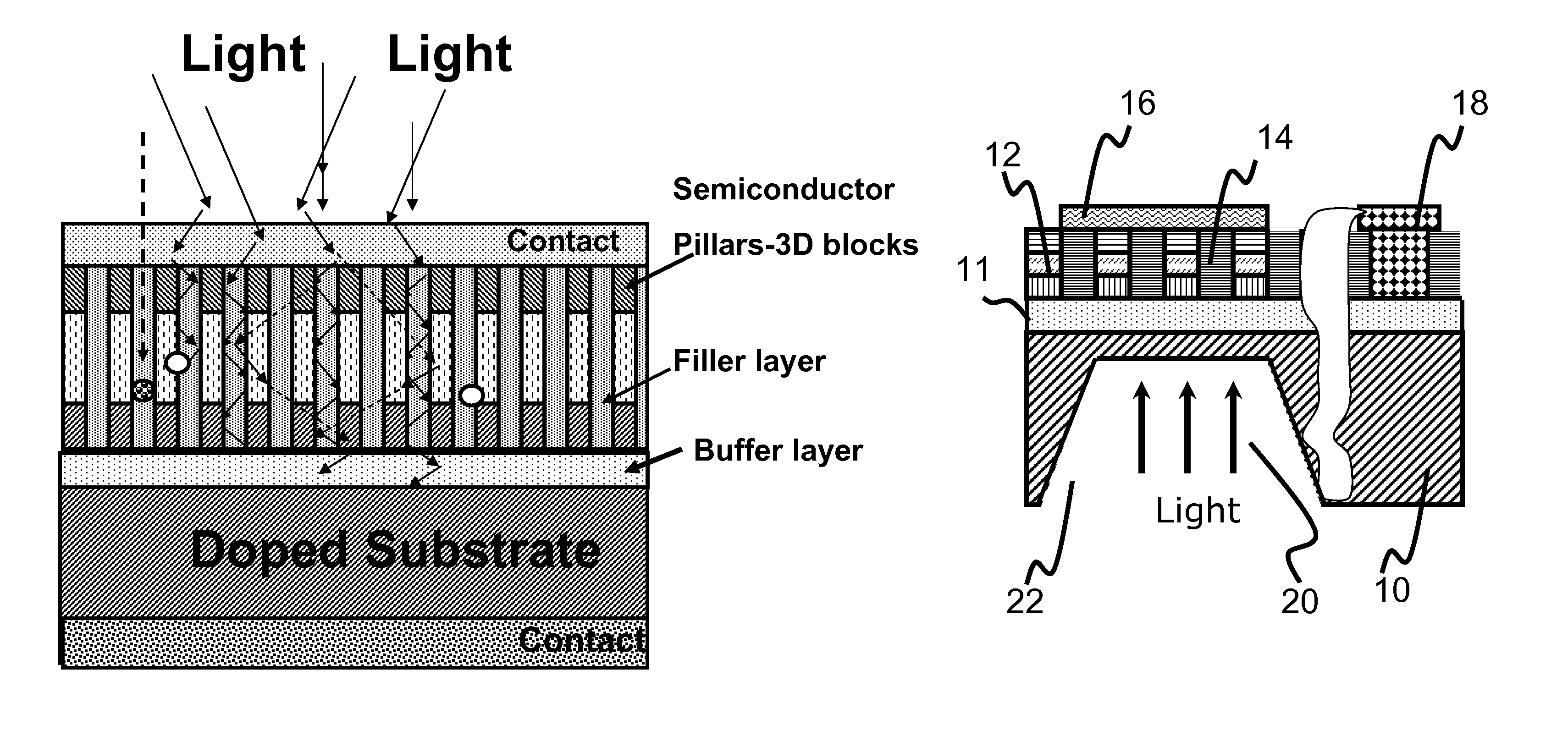
[0072]Here the structure and design we mention are for both top (also mentioned as ‘front’)-illuminated and bottom (also mentioned as ‘back’)-illuminated type detector and their array having broad spectral detection ranges. The main objective of this invention is to make the broad spectral detector and their array using the InGaAs using the InP substrate. This covers all photodiode and their array with broad spectral detection ranges from <300 nm to 3500 nm and also over, which uses the InGaAs as the absorption layer.

[0073]With changing the diode structure, spectral response is broadened as compared to its bulk material based photodiode. Similar diode structure c...


PUM


Abstract

This invention relates to photodetector and its array in the form of a image sensor having multispectral detection capability covering the wavelengths from ultra-violet (UV) or near UV to shortwave infrared (over 1700 nm), ultra-violet (UV) or near UV to mid infrared (3500 nm), or ultra-violet (UV) or near UV to 5500 nm. More particularly, this invention is related to the multicolor detector, which can detect the light wavelengths ranges from as low as UV to the wavelengths over 1700 nm covering the most of the communication wavelength, and also from UV to as high as 5500 nm using of the single monolithic detector fabricated on the single wafer. This invention is also related to the multispectral photodetector arrays for multicolor imaging, sensing, and advanced communication. Our innovative approach utilizes surface incident type (either top- or bottom-illuminated type) photodiode structure having single absorption layer and consisting of more than micro-nano-scaled 3-dimensional (3-D) blocks which can provide broader spectral response than that of the absorption layer made from the same type of material having macro-scaled structure.

Description

CROSS REFERENCE TO RELATED APPLICATIONS[0001]This application claims the benefit of U.S. Provisional Application No. 61 / 098,237 filed on Sep. 18, 2008.FIELD OF THE INVENTION[0002]This invention relates to photodetector and image sensor having multispectral detection capability covering the wavelengths from ultra-violet (UV) or near UV to mid infrared (3500 nm and also up to 5500 nm). More particularly, this invention is related to the multicolor detector, which can detect the light wavelengths ranges from as low as UV to the wavelengths as high as 3500 nm covering the most of the communication wavelength, and also from UV to as high as 5500 nm using of the single monolithic detector fabricated on the single wafer. This invention is also related to the multispectral photodetector arrays for multicolor imaging, sensing, and advanced communication.BACKGROUND OF THE INVENTION[0003]Solid-state imaging devices with higher resolution are used in many commercial applications especially came...

Claims


Application Information

Patent Timeline
IPC IPC(8): H01L33/00
CPCH01L31/035218H01L31/035227H01L31/035236B82Y20/00H01L27/14652H01L27/14694H01L27/14696H01L31/105H01L31/1013
Inventor DUTTA, ACHYUT KUMAR
Owner BANPIL PHOTONICS
Why Eureka
Try Eureka