Semiconductor device having interconnect structure for MIM capacitor and fuse elements

a technology of mim capacitor and fuse element, which is applied in the direction of semiconductor devices, semiconductor/solid-state device details, capacitors, etc., can solve the problems of poor manufacturing stability of conventional semiconductor devices, and achieve the effect of excellent manufacturing stability and reduced contact resistan

Active Publication Date: 2013-01-22
RENESAS ELECTRONICS CORP
View PDF8 Cites 2 Cited by
  • Summary
  • Abstract
  • Description
  • Claims
  • Application Information

AI Technical Summary

Benefits of technology

[0016]Since the connecting portion is in contact with the end portion of the conductive layer of the element in this invention, and a via does not penetrate through the element as in conventional cases, there is no need to form a via hole that penetrates through the conductive layer of the element. As described above, when a via hole that penetrates through the element is formed, the contact resistance between the via and the element varies or becomes higher. In this invention, on the other hand, there is no need to form a via hole that penetrates through the conductive layer of the element, and accordingly, a variation and an increase in the contact resistance can be prevented. Thus, a semiconductor device with excellent manufacturing stability can be obtained.
[0017]Also, since the connecting portion is in contact with the side face and upper face of the end portion of the conductive layer of the element in this embodiment, a sufficient contact area between the conductive layer of the element and the connecting portion can be secured. With this arrangement, the contact resistance between the connecting portion and the element can be made lower.
[0020]The present invention provides a semiconductor device that has excellent manufacturing stability and has lower contact resistance.

Problems solved by technology

However, the semiconductor devices disclosed in Japanese Laid-Open Patent Publication Nos. 2003-273220 and 2004-128498 have the following problems.
As described above, conventional semiconductor devices are poor in manufacturing stability.

Method used


Image

  • Semiconductor device having interconnect structure for MIM capacitor and fuse elements
  • Semiconductor device having interconnect structure for MIM capacitor and fuse elements
  • Semiconductor device having interconnect structure for MIM capacitor and fuse elements

Examples


first embodiment

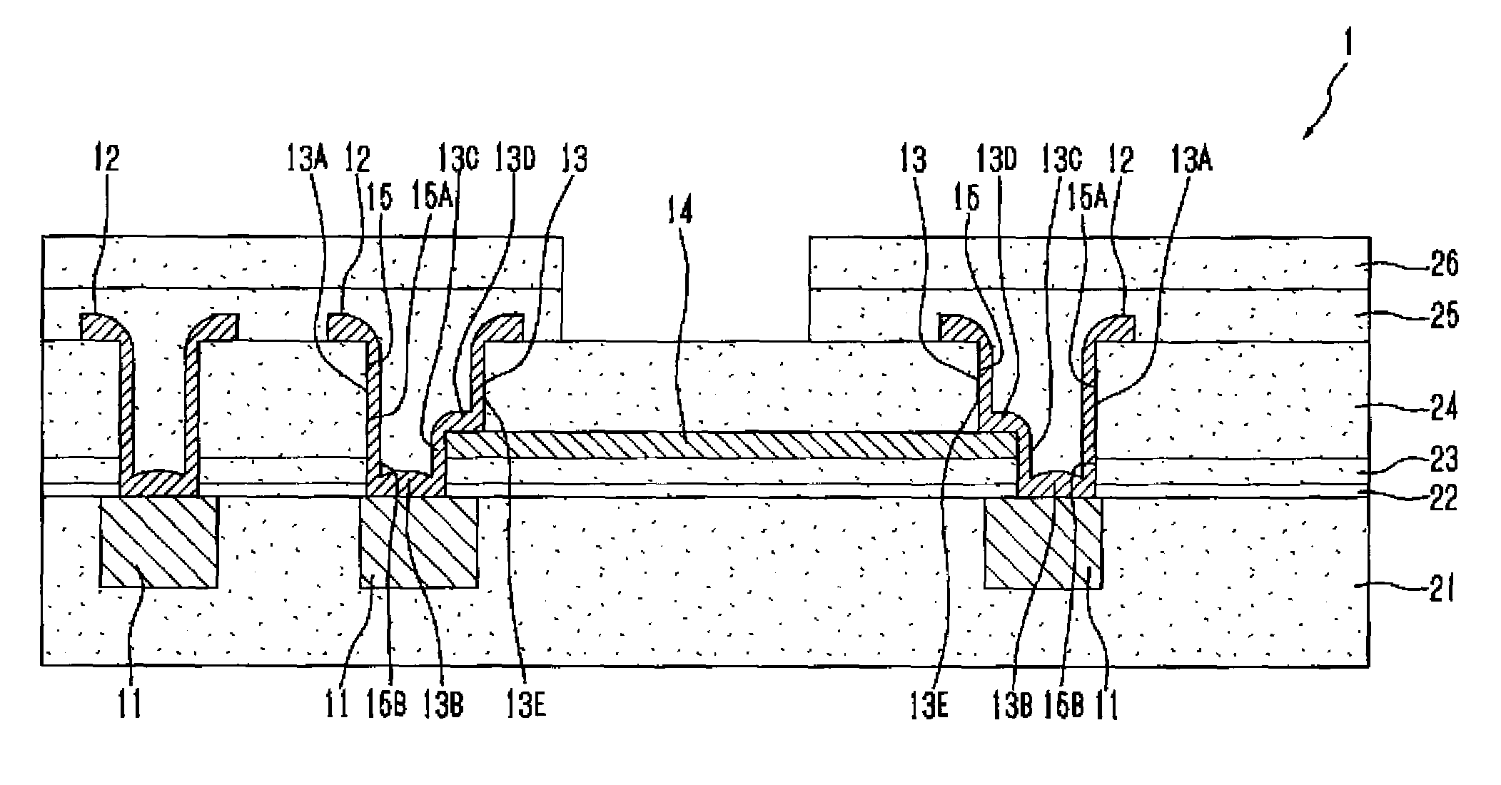
[0029]Referring to FIG. 1, a first embodiment of the present invention is briefly described.

[0030]A semiconductor device 1 of this embodiment includes an upper interconnect 12, a lower interconnect 11, insulating layers 22 through 24 that are placed between the upper interconnect 12 and the lower interconnect 11, a connecting portion 13 that is formed in the insulating layer 22 through 24 and connects the upper interconnect 12 to the lower interconnect 11, and an element 14 that is placed in the insulating layer 24 and has a conductive layer connected to the connecting portion 13.

[0031]The connecting portion 13 is placed over the lower interconnect 11 and the end portion of the conductive layer of the element 14. The connecting portions 13 is in contact with the upper face of the lower interconnect 11, the upper face of the end portion of the conductive layer of the element 14, and the side face of the end portion of the conductive layer of the element 14.

[0032]Referring now to FIG....

second embodiment

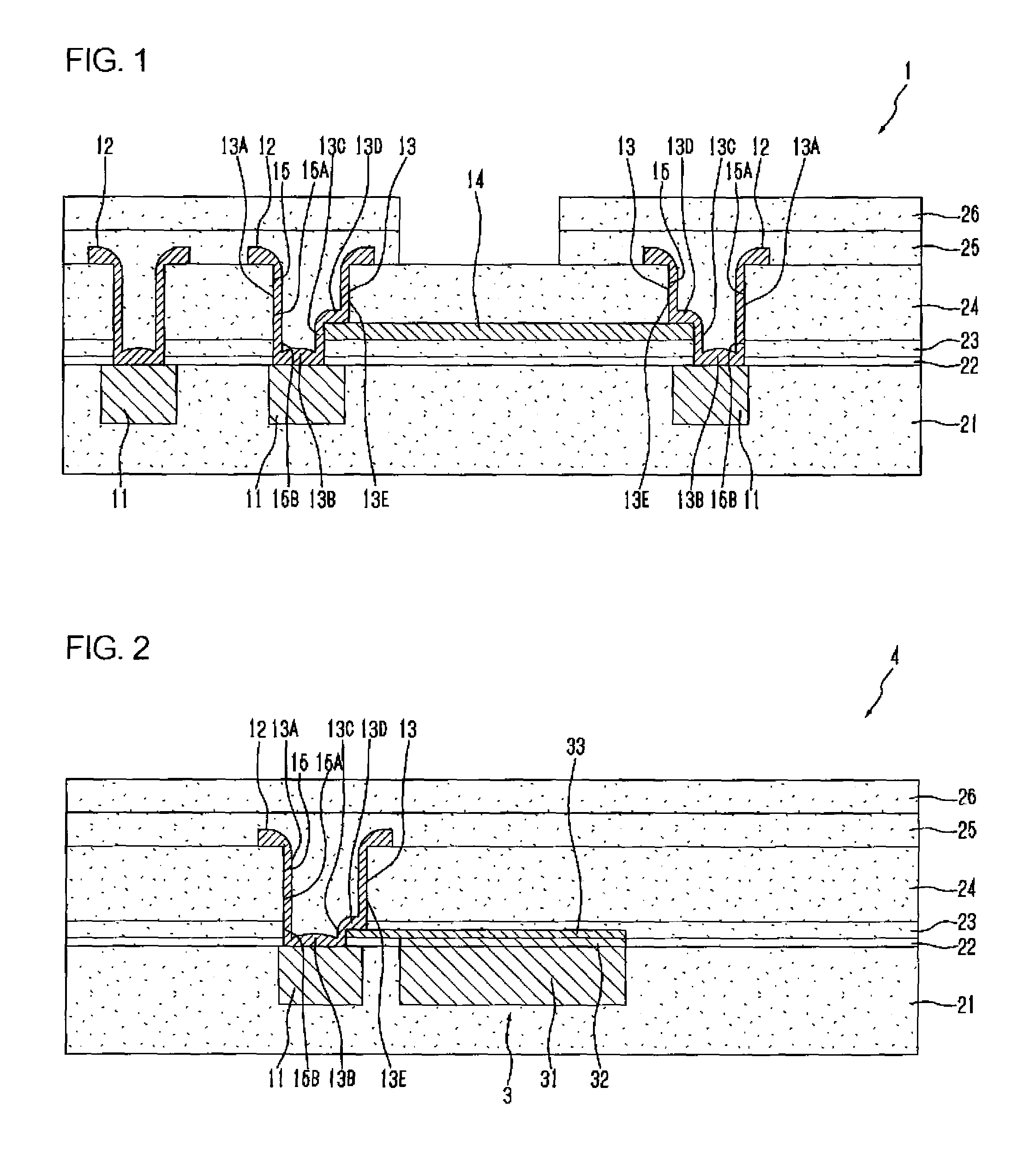
[0071]Referring to FIG. 2, a semiconductor device 4 of this embodiment is described.

[0072]In the foregoing embodiment, the element is the fuse element 14. In this embodiment, on the other hand, the element is a MIM (metal-insulator-metal) capacitor 3. The other aspects of this embodiment are the same as those of the foregoing embodiment.

[0073]The MIM capacitor 3 includes a lower electrode 31 that is formed in the first insulating layer 21, a dielectric film 32 that is provided on the lower electrode 31, and an upper electrode (a conductive layer) 33 that is provided on the dielectric film 32.

[0074]The lower electrode 31 is made of the same material as the lower interconnect 11, and may be made of copper, for example.

[0075]In this embodiment, the lower electrode 31 is made of the same material as the lower interconnect 11, but may be made of a different material from the lower electrode 31.

[0076]For example, the lower electrode 31 may be a metal film that is formed by stacking Ti, Ti...


PUM


Abstract

A semiconductor device includes an upper interconnect, a lower interconnect, insulating layers interposed between the upper interconnect and the lower interconnect, a connecting portion that is formed in the insulating layers and connects the upper interconnect and the lower interconnect, and an element that is placed in one of the insulating layers and has a conductive layer connected to the connecting portion. The connecting portion is formed over the lower interconnect and the end portions of the conductive layer of the element, and is in contact with the upper face of the lower interconnect and the upper faces and side faces of the end portions of the conductive layer of the element.

Description

[0001]This application is based on Japanese patent application No. 2008-289531, the content of which is incorporated herein by reference.BACKGROUND[0002]1. Technical Field[0003]The present invention relates to a semiconductor device.[0004]2. Related Art[0005]Conventionally, various elements are placed in the insulating layer interposed between the upper interconnects and the lower interconnects in a semiconductor device.[0006]Examples of the elements are fuse elements and MIM capacitors.[0007]Those elements are connected to vias in the insulating layers, and are connected to the upper interconnects and the lower interconnects through the vias (see Japanese Laid-Open Patent Publication Nos. 2003-273220 and 2004-128498, for example).[0008]More specifically, as shown in FIG. 4, vias 901 penetrate through an element 900 (a fuse element in this example), and the element 900 is in contact with the side faces of the vias 901. The upper end portions of the vias 901 are connected to upper in...

Claims


Application Information

Patent Timeline
Patent Type & Authority Patents(United States)
IPC IPC(8): H01L23/52
CPCH01L21/76877H01L23/5223H01L23/5258H01L23/5329H01L23/53295H01L28/60H01L2924/0002H01L2924/00
Inventor OSHIDA, DAISUKEKUNISHIMA, HIROYUKIOKADA, NORIO
Owner RENESAS ELECTRONICS CORP
Why Eureka
Try Eureka