A kind of organic/inorganic hybrid tin-lead mixed perovskite material and preparation method thereof
A perovskite material and perovskite technology are applied in semiconductor/solid-state device manufacturing, photovoltaic power generation, electrical components, etc., which can solve problems such as environmental hazards, low light absorption rate, and poor stability, and achieve reduced usage, light High absorption rate and good thermal stability
- Summary
- Abstract
- Description
- Claims
- Application Information
AI Technical Summary
Problems solved by technology
Method used
Image
Examples
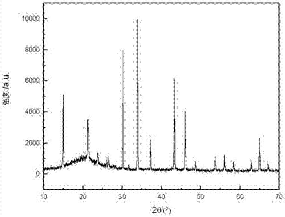
Embodiment 1
[0032] (1) Clean the substrate
[0033] Use FTO conductive glass with a thickness of 3mm as the substrate, first ultrasonically clean it in acetone for 12 minutes, then clean it in absolute ethanol for 12 minutes, and finally rinse it with deionized water and dry it;
[0034] (2) Preparation of reaction solution
[0035] Get 0.01mol of solid methyl ammonium bromide (CH 3 NH 3 Br) and 0.001mol solid lead bromide (PbBr 2 ) and 0.009mol solid tin bromide (SnBr 2 ), add 12mL of N,N-dimethylformamide (DMF) solution, stir until the solid powder is completely dissolved, and obtain a reaction solution, which is subjected to pulsed electromagnetic field treatment with a pulse voltage of 400V, a pulse frequency of 2Hz, and a pulse time of is 80s;
[0036] (3) Spin coating film formation
[0037] Drop the treated reaction solution on the conductive glass substrate, and perform low-speed spin-coating and high-speed spin-coating respectively with a homogenizer to form a perovskite fi...
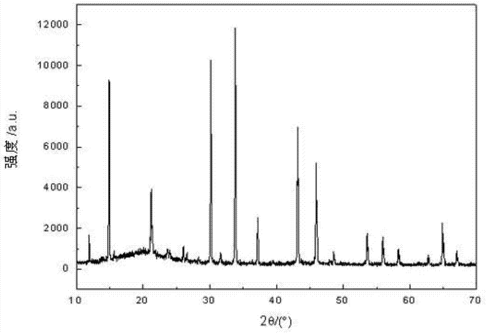
Embodiment 2
[0041] (1) Clean the substrate
[0042] Use FTO conductive glass with a thickness of 4mm as the substrate, first ultrasonically clean it in acetone for 14 minutes, then clean it in absolute ethanol for 14 minutes, and finally rinse it with deionized water and dry it;
[0043] (2) Preparation of reaction solution
[0044] Get 0.01mol of solid methyl ammonium bromide (CH 3 NH 3 Br) and 0.003mol solid lead bromide (PbBr 2 ) and 0.007mol solid tin bromide (SnBr 2), add 15mL of N,N-dimethylformamide (DMF) solution, stir until the solid powder is completely dissolved, and obtain a reaction solution, which is subjected to pulsed electromagnetic field treatment with a pulse voltage of 500V, a pulse frequency of 3Hz, and a pulse time of for 90s;
[0045] (3) Spin coating film formation
[0046] Drop the treated reaction solution on the conductive glass substrate, and perform low-speed spin-coating and high-speed spin-coating respectively with a homogenizer to form a perovskite fi...
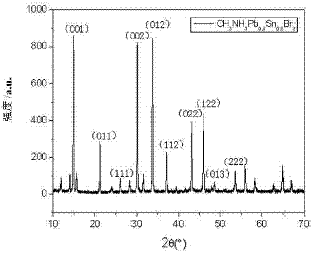
Embodiment 3
[0050] (1) Clean the substrate
[0051] Use FTO conductive glass with a thickness of 5mm as the substrate, first ultrasonically clean it in acetone for 16 minutes, then clean it in absolute ethanol for 16 minutes, and finally rinse it with deionized water and dry it;
[0052] (2) Preparation of reaction solution
[0053] Get 0.01mol of solid methyl ammonium bromide (CH 3 NH 3 Br) and 0.005mol solid lead bromide (PbBr 2 ) and 0.005mol solid tin bromide (SnBr 2 ), add 16mL of N,N-dimethylformamide (DMF) solution, stir until the solid powder is completely dissolved, and obtain a reaction solution, which is subjected to pulsed electromagnetic field treatment with a pulse voltage of 600V, a pulse frequency of 4Hz, and a pulse time of for 100s;
[0054] (3) Spin coating film formation
[0055] Add the pulse-treated reaction solution dropwise on the conductive glass substrate, and perform low-speed spin-coating and high-speed spin-coating with a homogenizer to form a perovskite...
PUM
 Abstract
Description
Claims
Application Information


