Face-up optical semiconductor device and method

a technology of optical semiconductor and face-up, which is applied in the direction of semiconductor devices, basic electric elements, electrical appliances, etc., can solve the problems of lowering light output, uneven light emission distribution, and small light extraction surface of optical semiconductor devices, so as to and reduce the weak light emission region

Active Publication Date: 2013-03-05
STANLEY ELECTRIC CO LTD
View PDF5 Cites 22 Cited by
  • Summary
  • Abstract
  • Description
  • Claims
  • Application Information

AI Technical Summary

Benefits of technology

[0024]The presently disclosed subject matter was devised in view of these and other problems and features and in association with the conventional art. According to an aspect of the presently disclosed subject matter, a face-up optical semiconductor device can include: a first semiconductor layer of a first conductive type; an active layer provided on the first semiconductor layer; a second semiconductor layer of a second conductive type provided on the active layer; a transparent electrode layer provided on the second semiconductor layer; a first electrode having a pad portion provided on any of the second semiconductor layer and the transparent electrode layer and an auxiliary electrode portion connected to the pad portion; a second electrode provided on an exposed region of the first semiconductor layer; and at least one outside independent electrode disposed adjacent to the transparent electrode layer and between the auxiliary electrode portion and the second electrode, the outside independent electrode being physically independent of the auxiliary electrode portion. The auxiliary electrode portion can be disposed on a first circle having a center located at the second electrode or on a tangent line of the first circle. The outside independent electrode can be disposed on a second circle having a center located at the second electrode or on a tangent line of the second circle so as to be an arc or linear electrode along the circle or the tangent line. A first radial distance between the first circle of the auxiliary electrode portion and the second circle of the outer independent electrode both having the center at the second electrode is smaller than a minimum value distance between the pad electrode of the first electrode and an area where a current density of a transparent electrode layer in a case where the optical semiconductor device does not have the outer independent electrode is minimum. This configuration can decrease the weak light emission region at the side regions of the optical semiconductor device.
[0026]The face-up optical semiconductor device according to the presently disclosed subject matter can further include at least one center independent electrode disposed between the auxiliary electrode portion and the second electrode. The center independent electrode can be disposed on a third circle having a center located at or adjacent the second electrode or a tangent line of the third circle so as to be along the third circle or the tangent line. This configuration can decrease the weak light emission region at the center of the optical semiconductor device.
[0027]The face-up optical semiconductor device according to the presently disclosed subject matter can further include at least one transparent insulation layer disposed between the auxiliary electrode portion and the outside independent electrode adjacent to the auxiliary electrode portion or adjacent two outside independent electrodes. The transparent insulation layer can be disposed on a fourth circle having a center located at or adjacent the second electrode or a tangent line of the fourth circle so as to be along the fourth circle or the tangent line. Furthermore, the transparent insulation layer can be formed to include an intersection between the fourth circle and a line connecting the center of the second electrode and an outside end portion of the auxiliary electrode portion or an outside end portion of the outside independent electrode near the first electrode out of the two outside independent electrodes. Furthermore, the total of the distance from the intersection to the outside end portion of the transparent insulation layer and a fourth radial distance between the first circle and the second circle on which the outside independent electrode adjacent to the auxiliary electrode portion is formed with the second electrode as a center, or a fifth radial distance between the two second circles on which the two adjacent outside independent electrodes are formed with the second electrode as a center, can be smaller than the minimum value distance. In this configuration, the transparent insulation layer can diffuse the current toward the outer sides of the device, thereby decreasing the weak light emission region at the side regions of the optical semiconductor device.
[0028]Furthermore, a transparent insulation layer similar to the previous insulation layer may be provided between the outside independent electrode and the center independent electrode. This transparent insulation layer can diffuse the current toward the center of the device, thereby decreasing the weak light emission region at the center portion of the optical semiconductor device.
[0029]In the above configuration, the outside independent electrode, the center independent electrode, and the transparent insulation layer can decrease the weak light emission region, thereby evening the light emission distribution. Namely, the outside independent electrode and / or the center independent electrode that is physically separated from the auxiliary electrode portion can be disposed between the first electrode and the second electrode. This configuration can substantially reduce the sheet electrode of the transparent electrode layer in a direction from the first electrode to the second electrode, whereby the current diffusion in this direction can be facilitated and the current density distribution, or the light emission distribution, can be evened. Furthermore, the outside independent electrode or the center independent electrode may be disposed on the same potential of electric field formed by the first electrode and the second electrode, thereby facilitating the current diffusion in the same potential direction and even the current density distribution, or the light emission distribution. In the above configuration, the transparent insulation layer can be formed near the end portions of the auxiliary electrodes, the outside independent electrodes, and the center independent electrode in order to adjust the diffusion direction of current, thereby evening the current diffusion over the entire optical semiconductor device. Accordingly, this configuration can even the light emission distribution.

Problems solved by technology

This means the light emission distribution may be concentrated on and near this line, resulting in uneven light emission distribution.
However, in this case, the light extracting surface of the optical semiconductor device may be small.
However, the area of the active layer per one optical semiconductor device, or the light emission region, is decreased by the removed active layer, thereby lowering the light output.
However, in this case the longitudinal size of the optical semiconductor device should be expanded, meaning that the distance between the p-side electrode 6 and the n-side electrode 7 may not be constant.
This may result in generation of current concentration region, which are not desirable.
This may result in uneven diffusion of current sufficiently to the end portion of the optical semiconductor device, i.e., the n-side electrode 7.
However, this method may have adverse effects such that, when the light passes through the transparent electrode layer 5, the amount of absorbed light may increase to lower the light extraction efficiency.
Furthermore, decreasing the sheet resistance lower than 5 Ω / sq. is quite difficult in terms of manufacturing.
In addition to this, the deposition process may require a longer time, thereby decreasing the yield in view of maintaining a uniform film thickness in the wafer and also increasing the manufacturing cost.
However, this method may increase the forward voltage in the optical semiconductor device.
This may result in reliability deterioration, such as disconnection of bonding wires, peeling off of the auxiliary electrode portions 62a and 62b, and the like, and decreased inner quantum efficiency may arise due to the increased current density.

Method used


Image

  • Face-up optical semiconductor device and method
  • Face-up optical semiconductor device and method
  • Face-up optical semiconductor device and method

Examples


Embodiment Construction

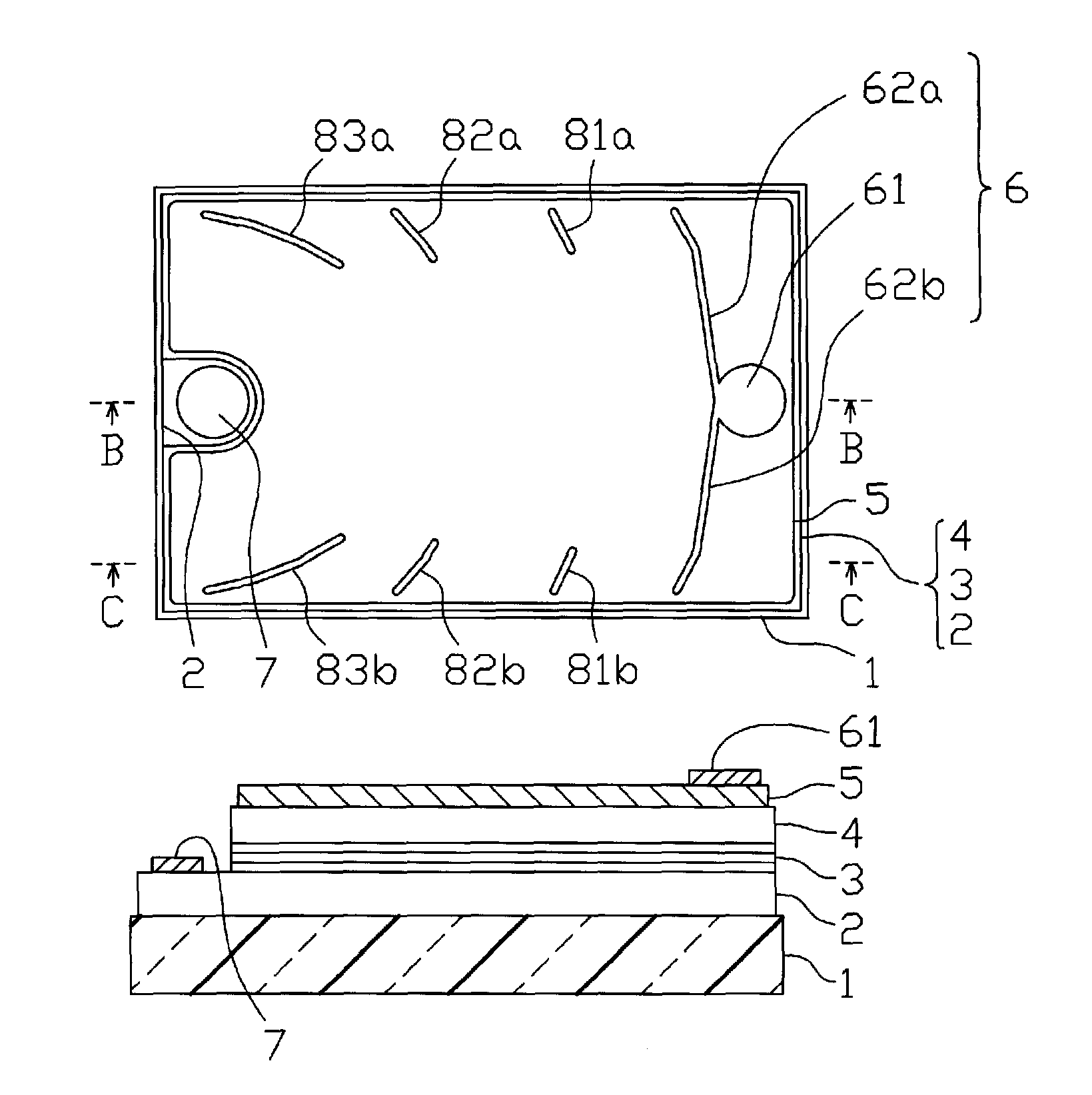
[0063]A description will now be made below to face-up optical semiconductor devices of the presently disclosed subject matter with reference to the accompanying drawings in accordance with exemplary embodiments.

[0064]FIG. 6 is a perspective view showing a first exemplary embodiment of a face-up optical semiconductor device made in accordance with principles of the presently disclosed subject matter. FIGS. 7A, 7B, and 7C are a top view, a cross sectional view taken along the line B-B in FIG. 7A, and a cross sectional view taken along the line C-C in FIG. 7A, respectively, showing the details of the face-up optical semiconductor device of FIG. 6.

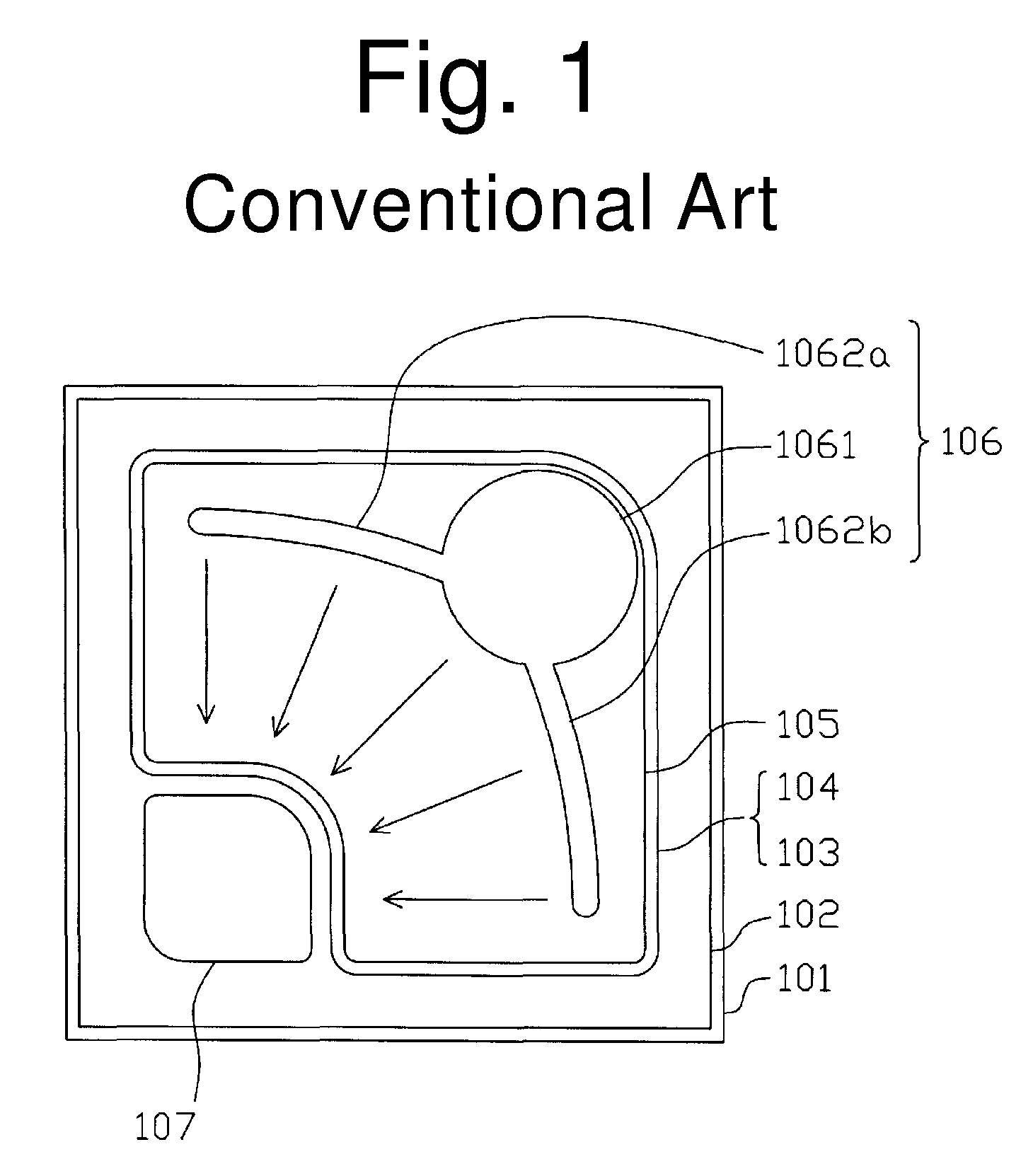
[0065]In FIGS. 6 and 7A to 7C, the basic configuration of the device can be similar to that of the conventional device of FIGS. 4A and 4B while the device can be provided with outside independent electrodes 81a, 81b, 82a, 82b, 83a, and 83b on the transparent electrode layer 5 at regions corresponding to the weak light emission regions 201a and...


PUM


Abstract

A face-up optical semiconductor device can be prepared by forming an n-type GaN layer, an active layer, and a p-type GaN layer on a C-plane sapphire substrate. Parts of the p-type GaN layer and the active layer can be removed, and a transparent electrode can be formed over all or most of the remaining p-type GaN layer. A p-side electrode including a pad portion and auxiliary electrode portions can be formed on the transparent electrode layer. An n-side electrode can be formed on the exposed n-type GaN layer. On regions of the transparent electrode layer where weak light emission regions may be formed, outside independent electrodes can be provided. They can be disposed on concentric circles with the n-side electrode as a center or tangent lines thereof so as to be along the circles or the tangent lines. The outside independent electrodes can diffuse current from the p-side electrode to the n-side electrode flowing through the transparent electrode layer into the short side end portions of the transparent electrode layer, thereby decreasing the weak light emission regions.

Description

[0001]This application claims the priority benefit under 35 U.S.C. §119 of Japanese Patent Applications No. 2009-292068 filed on Dec. 24, 2009 and No. 2010-147349 filed on Jun. 29, 2010, which are hereby incorporated in their entirety by reference.TECHNICAL FIELD[0002]The presently disclosed subject matter relates to an optical semiconductor device such as a light emitting diode (LED) and the like, and in particular, to a face-up optical semiconductor device.BACKGROUND ART[0003]Common face-up optical semiconductor devices can be configured to include various semiconductor layers (including an n-type semiconductor layer formed on an insulative growth substrate, and an active layer serving as a light emitting layer, and a p-type semiconductor layer), a transparent electrode layer, a p-side electrode formed on the transparent electrode, and an n-side electrode formed on an exposed portion of the n-type semiconductor layer. Here, the transparent electrode layer can be formed on an entir...

Claims


Application Information

Patent Timeline
Patent Type & Authority Patents(United States)
IPC IPC(8): H01L33/38
CPCH01L33/38H01L2933/0016H01L33/42
Inventor TANAKA, SATOSHIYOKOBAYASHI, YUSUKE
Owner STANLEY ELECTRIC CO LTD
Why Eureka
Try Eureka