[0024]The presently disclosed
subject matter was devised in view of these and other problems and features and in association with the conventional art. According to an aspect of the presently disclosed
subject matter, a face-up optical semiconductor device can include: a first semiconductor layer of a first conductive type; an active layer provided on the first semiconductor layer; a second semiconductor layer of a second conductive type provided on the active layer; a transparent electrode layer provided on the second semiconductor layer; a first electrode having a pad portion provided on any of the second semiconductor layer and the transparent electrode layer and an
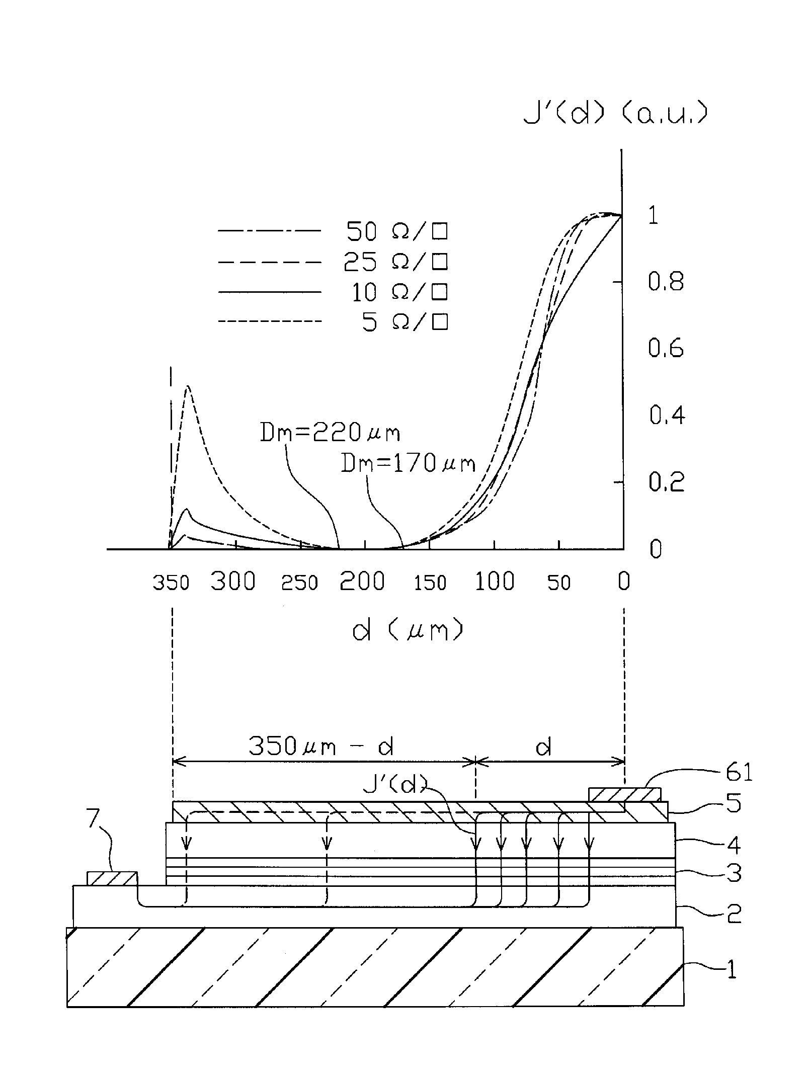
auxiliary electrode portion connected to the pad portion; a second electrode provided on an exposed region of the first semiconductor layer; and at least one outside independent electrode disposed adjacent to the transparent electrode layer and between the auxiliary electrode portion and the second electrode, the outside independent electrode being physically independent of the auxiliary electrode portion. The auxiliary electrode portion can be disposed on a first circle having a center located at the second electrode or on a tangent line of the first circle. The outside independent electrode can be disposed on a second circle having a center located at the second electrode or on a tangent line of the second circle so as to be an arc or linear electrode along the circle or the tangent line. A first radial distance between the first circle of the auxiliary electrode portion and the second circle of the outer independent electrode both having the center at the second electrode is smaller than a minimum value distance between the pad electrode of the first electrode and an area where a
current density of a transparent electrode layer in a case where the optical semiconductor device does not have the outer independent electrode is minimum. This configuration can decrease the weak light emission region at the side regions of the optical semiconductor device.
[0026]The face-up optical semiconductor device according to the presently disclosed subject matter can further include at least one center independent electrode disposed between the auxiliary electrode portion and the second electrode. The center independent electrode can be disposed on a third circle having a center located at or adjacent the second electrode or a tangent line of the third circle so as to be along the third circle or the tangent line. This configuration can decrease the weak light emission region at the center of the optical semiconductor device.
[0027]The face-up optical semiconductor device according to the presently disclosed subject matter can further include at least one transparent
insulation layer disposed between the auxiliary electrode portion and the outside independent electrode adjacent to the auxiliary electrode portion or adjacent two outside independent electrodes. The transparent
insulation layer can be disposed on a fourth circle having a center located at or adjacent the second electrode or a tangent line of the fourth circle so as to be along the fourth circle or the tangent line. Furthermore, the transparent
insulation layer can be formed to include an intersection between the fourth circle and a line connecting the center of the second electrode and an outside end portion of the auxiliary electrode portion or an outside end portion of the outside independent electrode near the first electrode out of the two outside independent electrodes. Furthermore, the total of the distance from the intersection to the outside end portion of the transparent insulation layer and a fourth radial distance between the first circle and the second circle on which the outside independent electrode adjacent to the auxiliary electrode portion is formed with the second electrode as a center, or a fifth radial distance between the two second circles on which the two adjacent outside independent electrodes are formed with the second electrode as a center, can be smaller than the minimum value distance. In this configuration, the transparent insulation layer can diffuse the current toward the outer sides of the device, thereby decreasing the weak light emission region at the side regions of the optical semiconductor device.
[0028]Furthermore, a transparent insulation layer similar to the previous insulation layer may be provided between the outside independent electrode and the center independent electrode. This transparent insulation layer can diffuse the current toward the center of the device, thereby decreasing the weak light emission region at the center portion of the optical semiconductor device.
[0029]In the above configuration, the outside independent electrode, the center independent electrode, and the transparent insulation layer can decrease the weak light emission region, thereby
evening the light emission distribution. Namely, the outside independent electrode and / or the center independent electrode that is physically separated from the auxiliary electrode portion can be disposed between the first electrode and the second electrode. This configuration can substantially reduce the sheet electrode of the transparent electrode layer in a direction from the first electrode to the second electrode, whereby the current
diffusion in this direction can be facilitated and the
current density distribution, or the light emission distribution, can be evened. Furthermore, the outside independent electrode or the center independent electrode may be disposed on the same potential of
electric field formed by the first electrode and the second electrode, thereby facilitating the current
diffusion in the same potential direction and even the
current density distribution, or the light emission distribution. In the above configuration, the transparent insulation layer can be formed near the end portions of the auxiliary electrodes, the outside independent electrodes, and the center independent electrode in order to adjust the diffusion direction of current, thereby
evening the current diffusion over the entire optical semiconductor device. Accordingly, this configuration can even the light emission distribution.


