On-chip memory testing

a technology of flash memory and on-chip memory, applied in the direction of digital storage, discharge tube testing, instruments, etc., can solve the problem of limited flash access

Active Publication Date: 2013-03-05
TEXAS INSTR INC
View PDF6 Cites 4 Cited by
  • Summary
  • Abstract
  • Description
  • Claims
  • Application Information

AI Technical Summary

Problems solved by technology

Flash access is limited by device architecture which presents potential gaps where equal access and comparison cannot be made to all portions of the memory.

Method used


Image

  • On-chip memory testing
  • On-chip memory testing
  • On-chip memory testing

Examples


Embodiment Construction

[0015]Specific embodiments of the invention will now be described in detail with reference to the accompanying figures. Like elements in the various figures are denoted by like reference numerals for consistency. In the following detailed description of embodiments of the invention, numerous specific details are set forth in order to provide a more thorough understanding of the invention. However, it will be apparent to one of ordinary skill in the art that the invention may be practiced without these specific details. In other instances, well-known features have not been described in detail to avoid unnecessarily complicating the description.

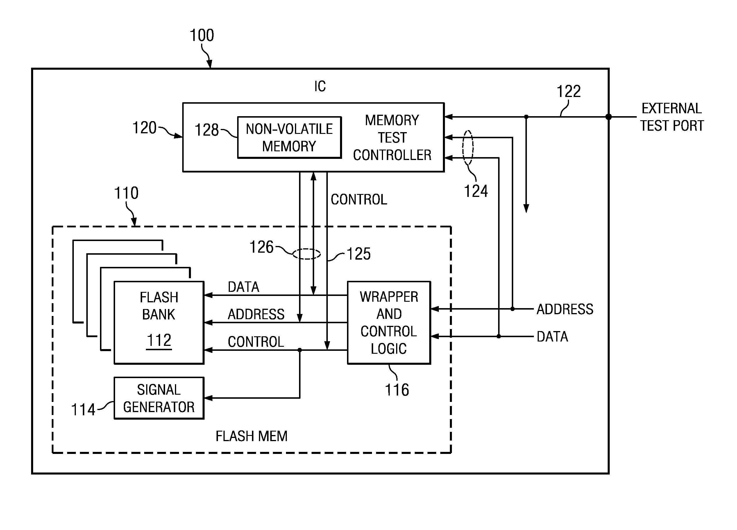
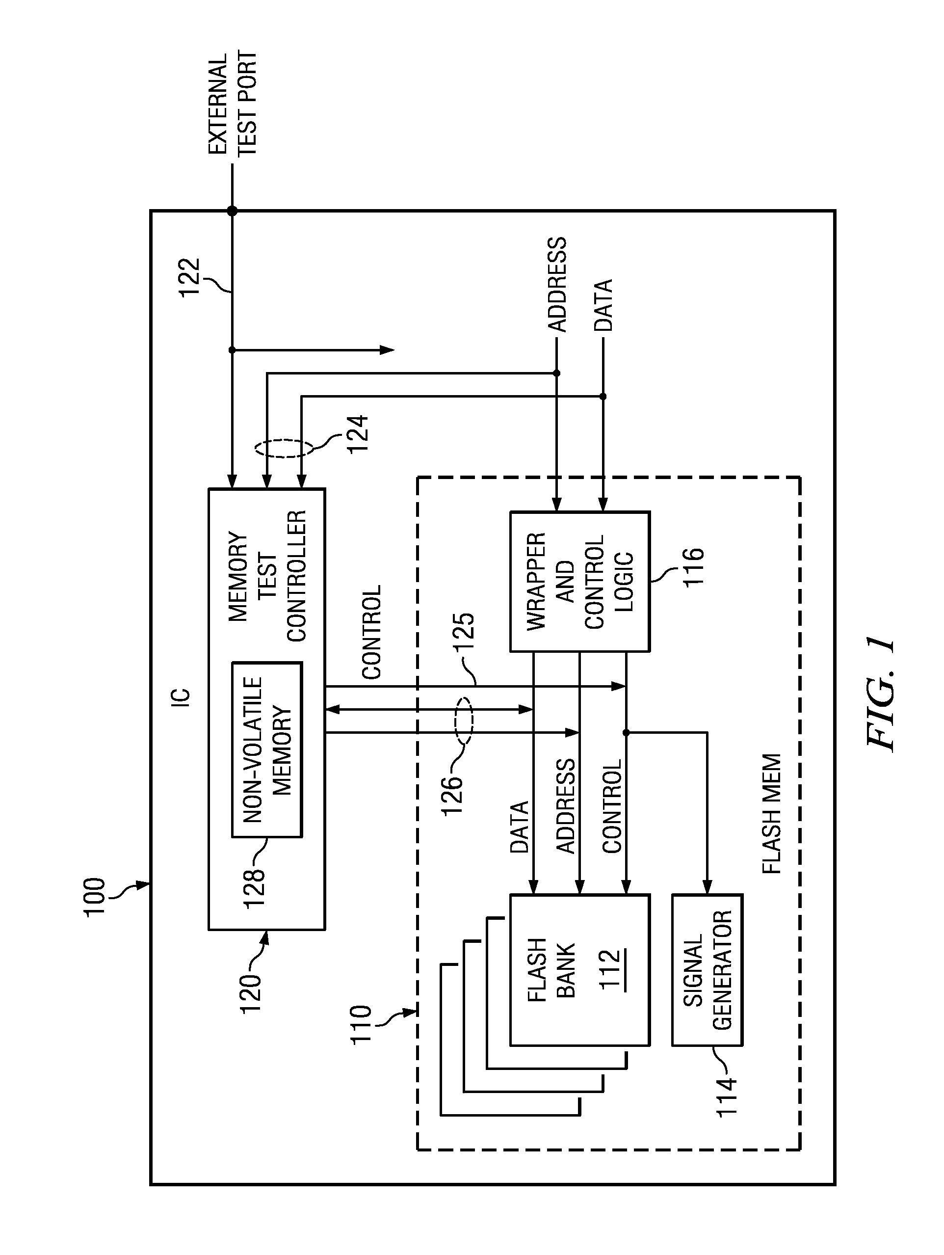
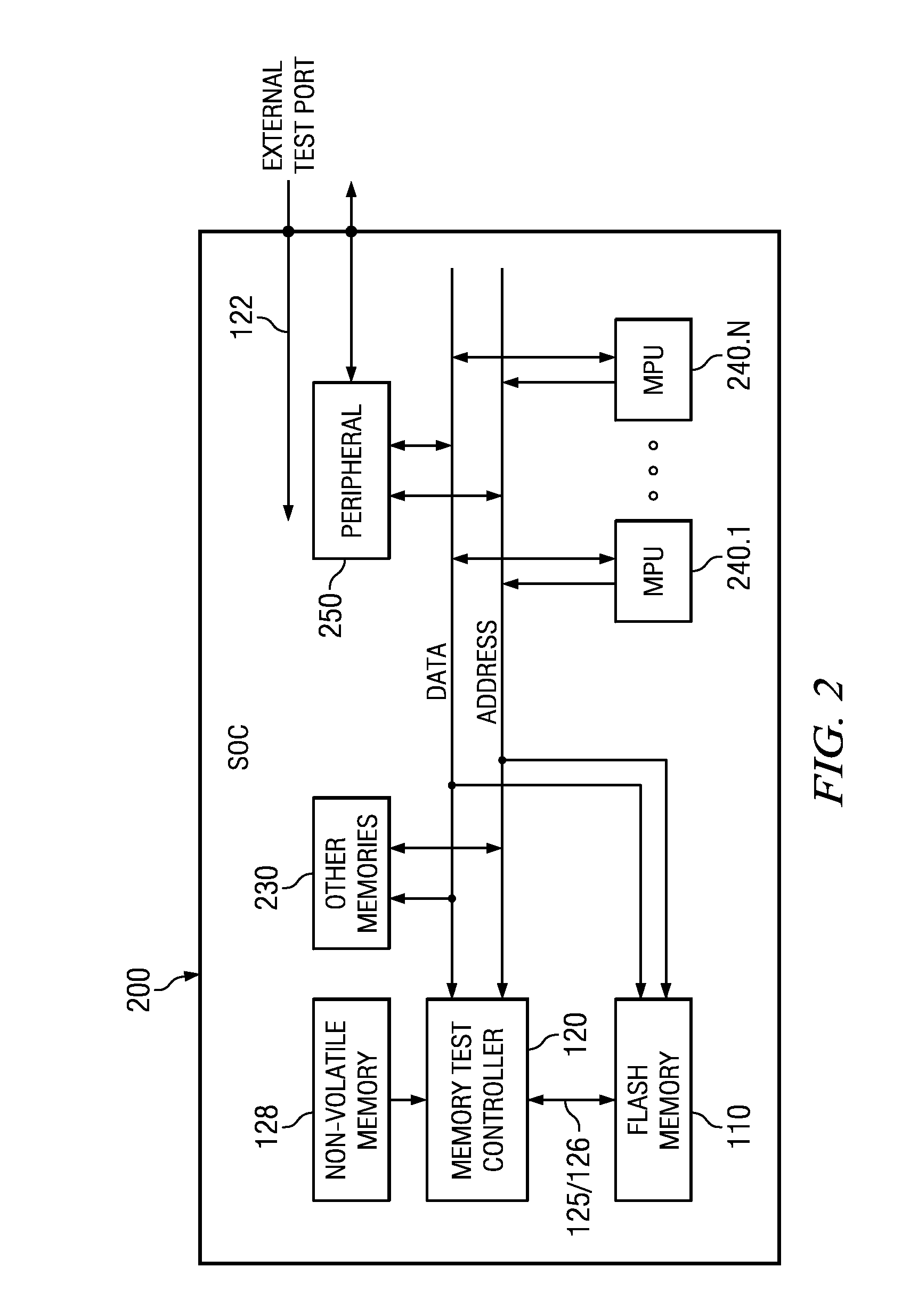
[0016]To address the quality, portability and test cost associated with embedded flash manufacture, embodiments of the present invention may have a flash memory array in an integrated circuit and include an on-chip test controller that is coupled to provide an address to the flash memory array and to read and write a full row at the provided ad...


PUM


Abstract

An integrated circuit is described that has a substrate with a memory array with dedicated support hardware formed on the substrate. An access wrapper circuit is coupled to address and data lines of the memory array and to control lines of the dedicated support hardware. The wrapper circuit is configured to provide an access port to the memory array. A test controller is formed on the substrate and coupled in parallel with the access wrapper circuit to the address and data lines of the memory array and to the control lines of the dedicated support hardware, wherein the test controller is operable to perform a test of the memory array by manipulating control signals to the support hardware in addition to those required to write data patterns into the memory array and to read the contents of the memory array.

Description

FIELD OF THE INVENTION[0001]This invention generally relates to testing of integrated circuits, and in particular to testing of flash memory arrays in an integrated circuit.BACKGROUND OF THE INVENTION[0002]Flash memory is a non-volatile computer storage technology that can be electrically erased and reprogrammed. It is primarily used in memory cards, USB flash drives, and solid-state drives for general storage and transfer of data between computers and other digital products. It is a specific type of EEPROM (electrically-erasable programmable read-only memory) that is erased and programmed in large blocks. Because erase cycles are slow, the large block sizes used in flash memory erasing give it a significant speed advantage over old-style EEPROM when writing large amounts of data.[0003]Since flash memory is non-volatile, no power is needed to maintain the information stored in the chip. In addition, flash memory offers fast read access times (although not as fast as volatile DRAM me...

Claims


Application Information

Patent Timeline
Patent Type & Authority Patents(United States)
IPC IPC(8): G01R31/24
CPCG11C29/00G11C29/16G11C16/00G11C2029/0401
Inventor BURGGRAF, III, DANIEL ROBERTPENDURTY, HARI
Owner TEXAS INSTR INC
Why Eureka
Try Eureka