

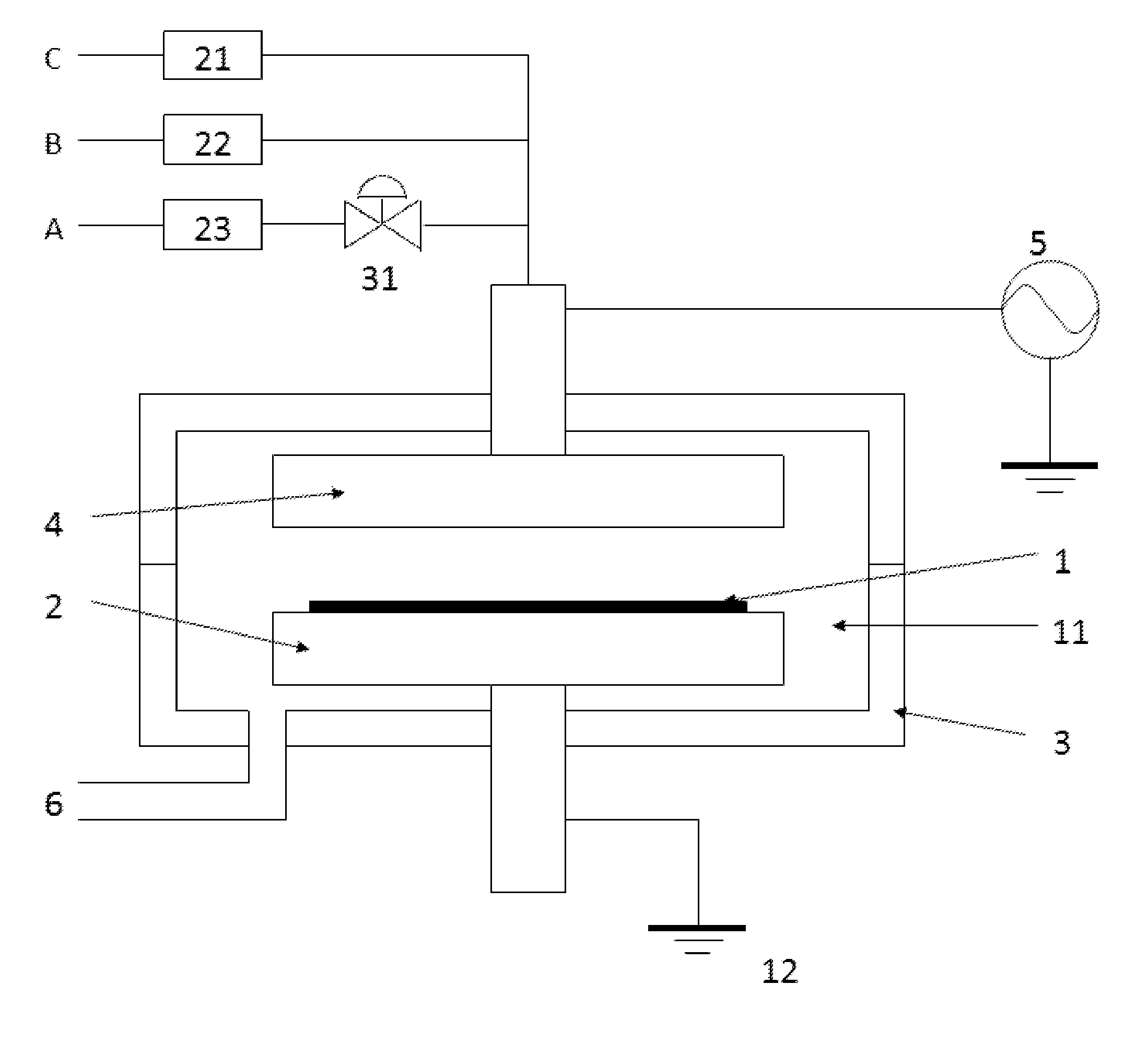
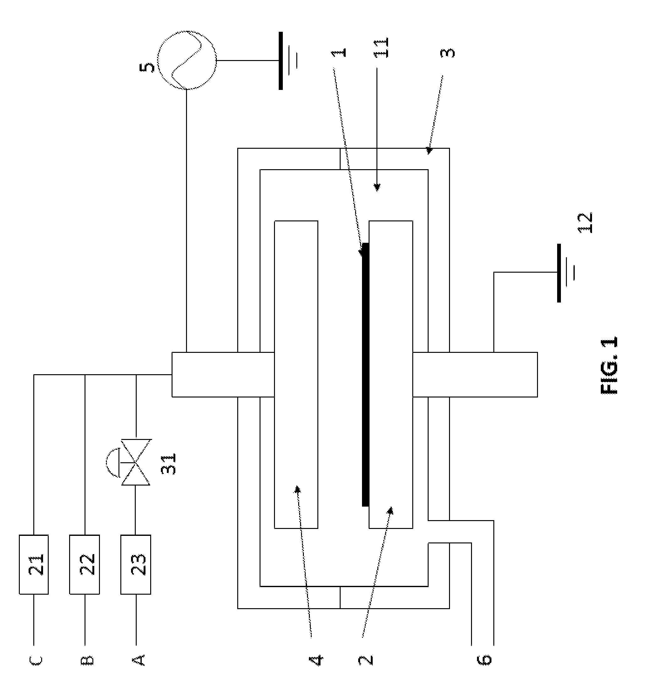
Method of forming conformal film having si-N bonds on high-aspect ratio pattern
a technology of conformal film and high-aspect ratio, applied in the direction of coating, chemical vapor deposition coating, plasma technique, etc., can solve the problems of poor conformality or poor step coverage on a substrate containing small and/or high aspect ratio features, poor conformal coverage can hamper the development of higher density circuit devices and elements, etc., to improve the conformality or step coverage of the film, increase the mobility and diffusivity of molecules on the surface, and improve the effect of conformality
- Summary
- Abstract
- Description
- Claims
- Application Information
AI Technical Summary
Benefits of technology
Problems solved by technology
Method used
Image

Examples
example 3
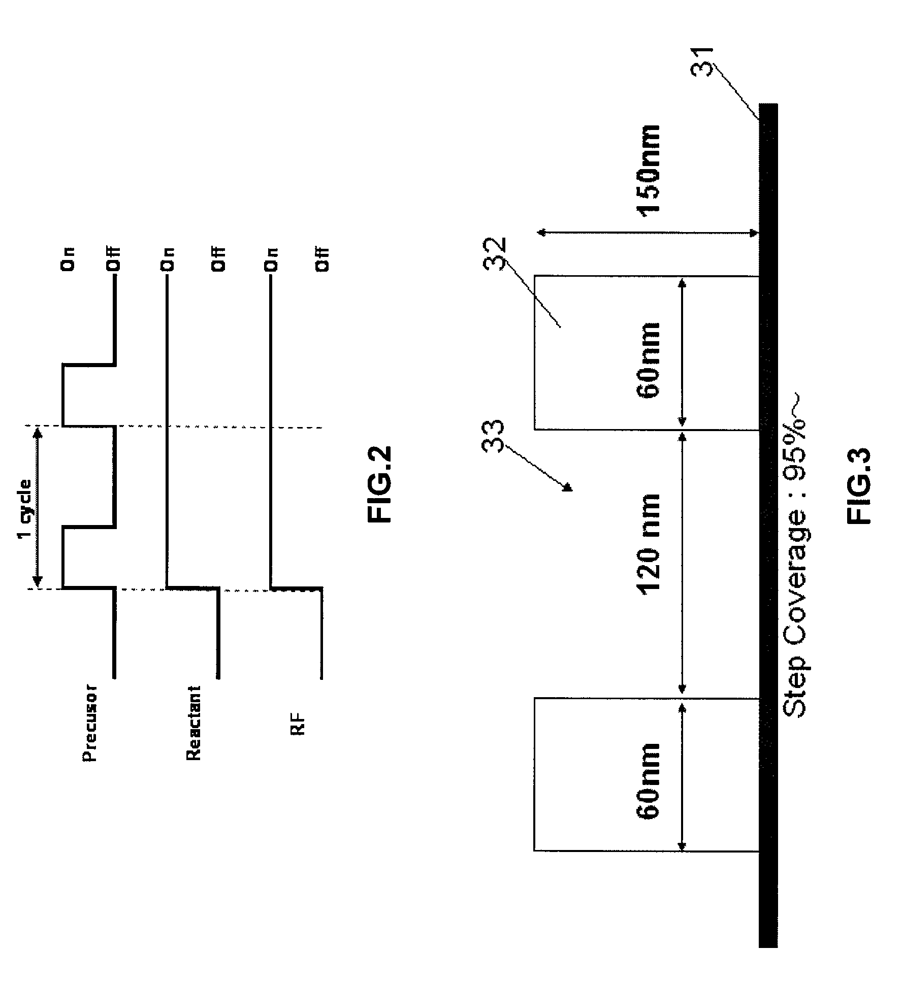
[0083]Under the same conditions as in Example 1, except for the pressure, a SiCN layer was formed on the substrate with the trenches having an aspect ratio of 2.5. The pressure was 600 Pa. After completion of the deposition, the trenches were observed with a scanning electron microscope (SEM) and the conformality was determined.
[0084]The results are shown in Table 2 below.
[0085]
TABLE 2ConformalityPressure (Pa)300 (Example 1)600 (Example 3)Conformality95%89%
[0086]As shown in Table 2, in Example 3, when the pressure was higher (Example 3), the conformality was not as good as that when the pressure was low (Example 1). However, the conformality in Example 3 was significantly superior to that in Comparative Example 1 since the RF power was applied in two steps as in Example 1.
[0087]A significant advantage of the method of at least one of the disclosed embodiments of the present invention is that highly-conformal silicon nitride layers or other Si—N dielectric layers can be formed on var...
PUM
| Property | Measurement | Unit |
|---|---|---|
| aspect ratio | aaaaa | aaaaa |
| pressure | aaaaa | aaaaa |
| temperatures | aaaaa | aaaaa |
Abstract
Description
Claims
Application Information