

Atomic layer deposition of high k metal silicates
a technology of metal silicates and atomic layers, applied in chemical vapor deposition coatings, coatings, solid-state devices, etc., can solve the problems of increasing the requirements of advanced thin films, reducing the and insulators now being thin, etc. , to achieve the effect of reducing carbon contamination, reducing carbon contamination, and reducing the required operating temperature of ald processes
- Summary
- Abstract
- Description
- Claims
- Application Information
AI Technical Summary
Benefits of technology
Problems solved by technology
Method used
Image

Examples
Embodiment Construction
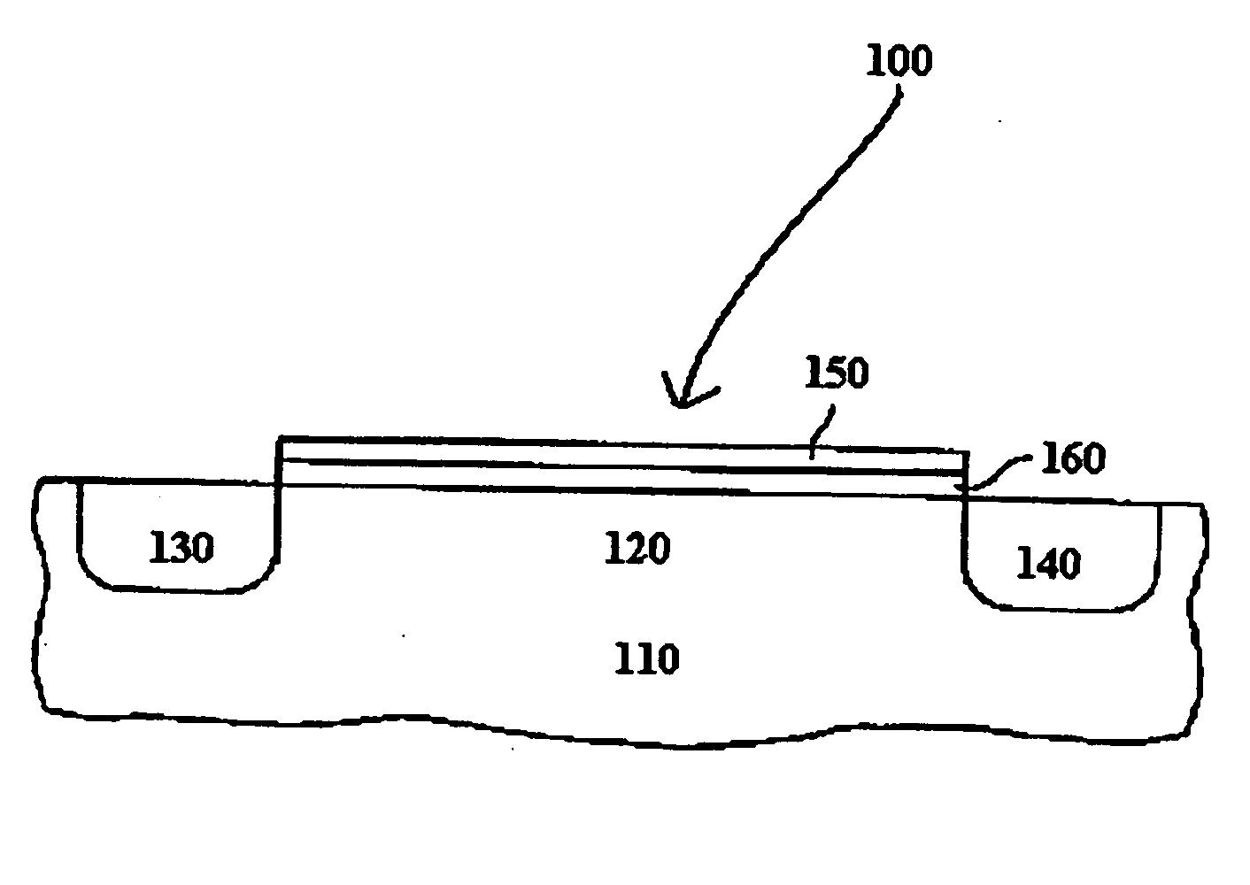
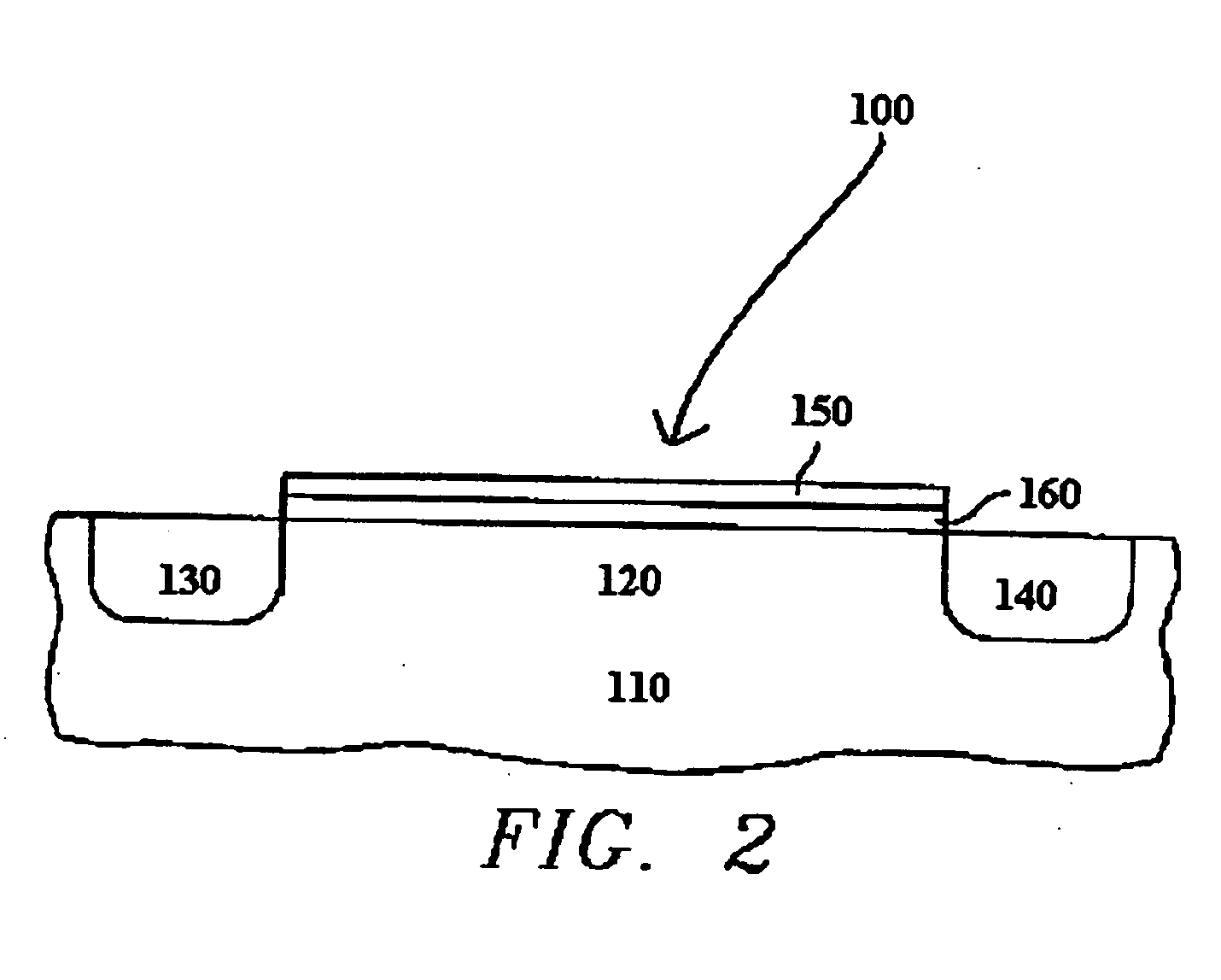
[0017] The invention provides ALD processes for forming high k metal silicates to replace silicon dioxide in gate and / or capacitor dielectric applications. A preferred metal silicate formed according to the process is hafnium silicate. Hafnium silicate exhibits superior thermal stability and, thereby, results in less interfacial silicon dioxide growth, compared to other silicates.
[0018] Prior to starting the pulse cycle, a substrate, generally a silicon wafer, is placed into a reaction chamber, often through a valve located at one end of the chamber. Preferably, the silicon wafer has been cleaned with hydrogen fluoride to remove native silicon dioxide.
[0019] The substrate sits on a heatable wafer holder that supports and heats the substrate to the desired reaction temperature. Once the substrate is properly positioned, the pulse cycle can begin.
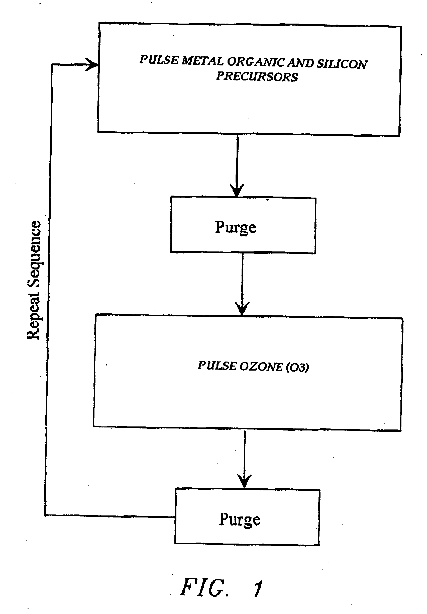
[0020] Generally, prior to the first pulse in the pulse cycle, the wafer is heated to a temperature ranging from about 100° C. to about 5...
PUM
| Property | Measurement | Unit |
|---|---|---|
| Dielectric polarization enthalpy | aaaaa | aaaaa |
Abstract
Description
Claims
Application Information