

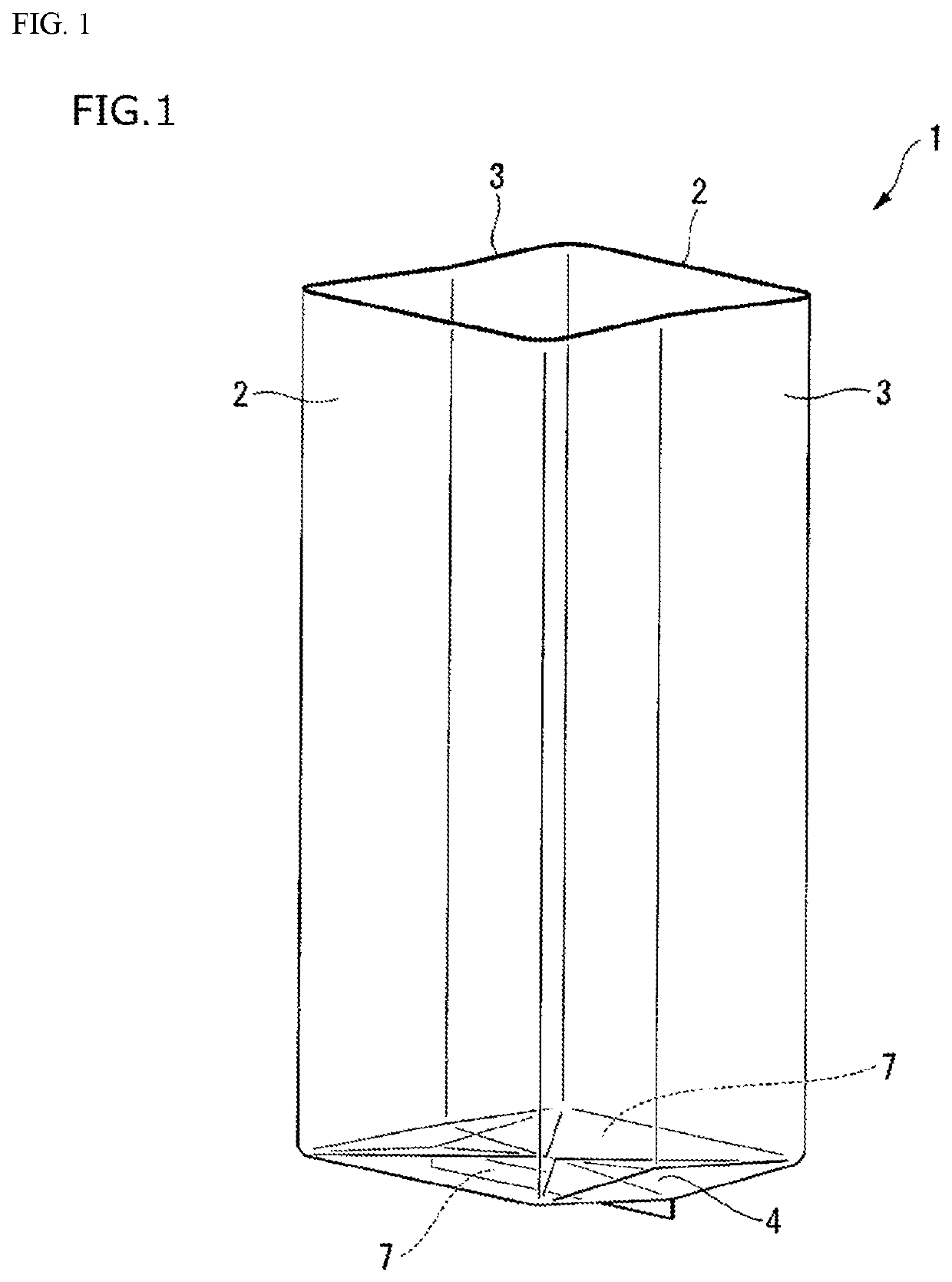
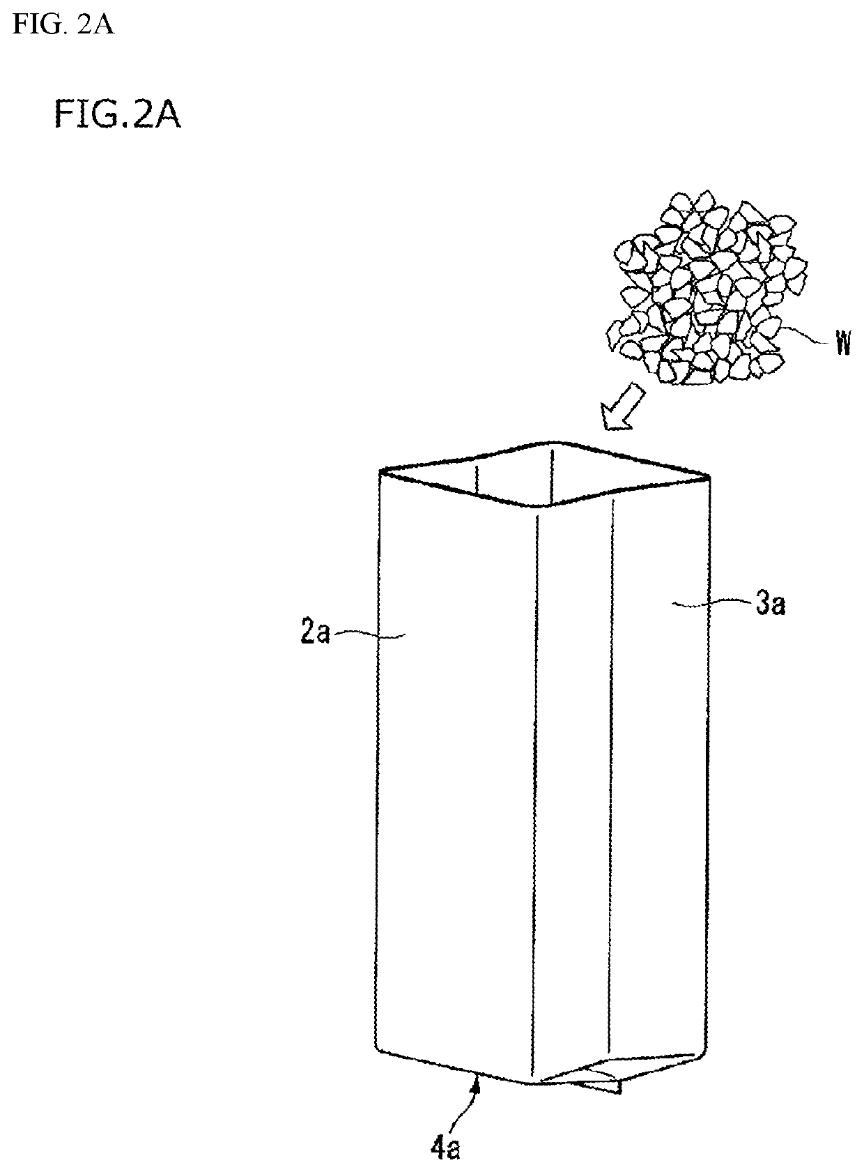
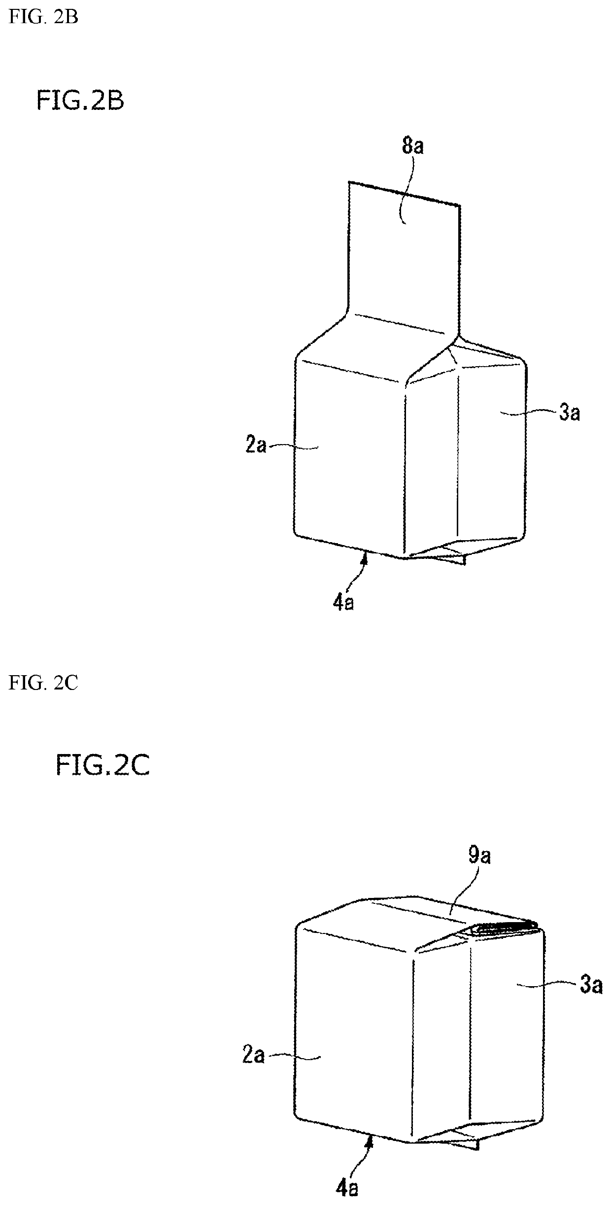
Packaging method for polycrystalline silicon, double-packaging method for polycrystalline silicon, and producing method of raw material for monocrystalline silicon
a polycrystalline silicon and polycrystalline silicon technology, applied in the direction of packaging, transportation and packaging, silicon compounds, etc., can solve the problems of insufficient reduction of surface carbon impurities and more severe requirements for polycrystalline silicon quality, so as to reduce the contamination of organic impurities, and reduce the concentration of carbon impurities
- Summary
- Abstract
- Description
- Claims
- Application Information
AI Technical Summary
Benefits of technology
Problems solved by technology
Method used
Image

Examples
examples
[0088]Polyethylene bags having a thickness of about 0.3 mm and a width about 140 mm are used as the packaging bags, filled with polycrystalline silicon lumps, and heat-sealed using an impulse sealer (MTB-25 made by Tsubakimoto Kogyo Co., Ltd). Regarding the polycrystalline silicon lumps, three lumps having a maximum side length of 20 mm to 50 mm are put on a Petri dish made of glass, and stored in the packaging bag. In order to exclude a possibility that contaminants originated from organic substance are adhered on the surface of the polycrystalline silicon lumps, the Petri dish on which a cleansing treatment is carried out are put together in an electric furnace as a pretreatment, and a heating treatment is carried out at about 500° C. for about 120 minutes. Thereby, in a case in which impurities originated from organic substance are adhered on the surface of the polycrystalline silicon lumps, most of that is volatilized and removed.
[0089]Pretreated polycrystalline silicon lumps ar...
PUM
| Property | Measurement | Unit |
|---|---|---|
| temperature | aaaaa | aaaaa |
| width | aaaaa | aaaaa |
| thickness | aaaaa | aaaaa |
Abstract
Description
Claims
Application Information