Method of depositing dielectric film by ALD using precursor containing silicon, hydrocarbon, and halogen

a dielectric film and precursor technology, applied in the direction of coatings, chemical vapor deposition coatings, metallic material coating processes, etc., can solve the problems of poor coverage, varying film qualities at different parts of the pattern, etc., and achieve high conformality and reduce the effect of substitution reactions such as carbonization and nitridation

Active Publication Date: 2012-12-11
ASM JAPAN
View PDF7 Cites 429 Cited by
  • Summary
  • Abstract
  • Description
  • Claims
  • Application Information

AI Technical Summary

Benefits of technology

[0012]By using the above precursors, replacement reaction such as carbonization and nitridation can substantially be improved, thereby enabling the formation of a film having desired components without substantial contamination and having high conformality (e.g., at least about 90%, or at least about 95%) even for an irregular surface having an aspect ratio of about one or higher (e.g., about 1 to about 10, or about 2 to about 5).

Problems solved by technology

While the SiO process involving oxidizing replacement is basically insensitive to effects of temperature, etc., and thus can be performed at relatively low temperatures to form film, the SiN process requires high temperatures for film to be formed because nitriding replacement does not occur easily due to the skeleton of the material used in this process, and as wiring patterns become finer, drop in replacement efficiency in the pattern and other undesirable outcomes lead to varying film qualities at different parts of the pattern as well as poor coverage.

Method used


Image

  • Method of depositing dielectric film by ALD using precursor containing silicon, hydrocarbon, and halogen
  • Method of depositing dielectric film by ALD using precursor containing silicon, hydrocarbon, and halogen
  • Method of depositing dielectric film by ALD using precursor containing silicon, hydrocarbon, and halogen

Examples


example

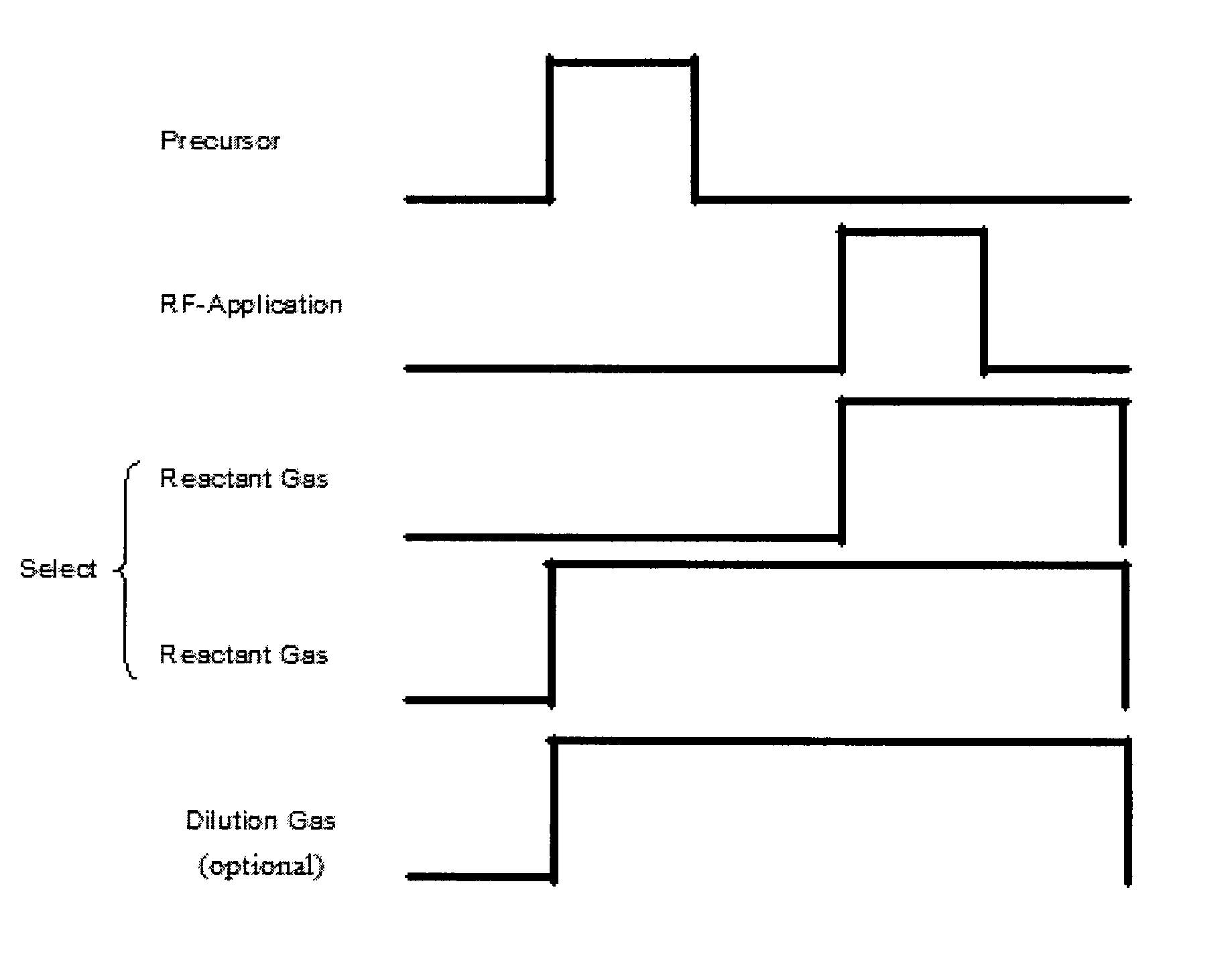
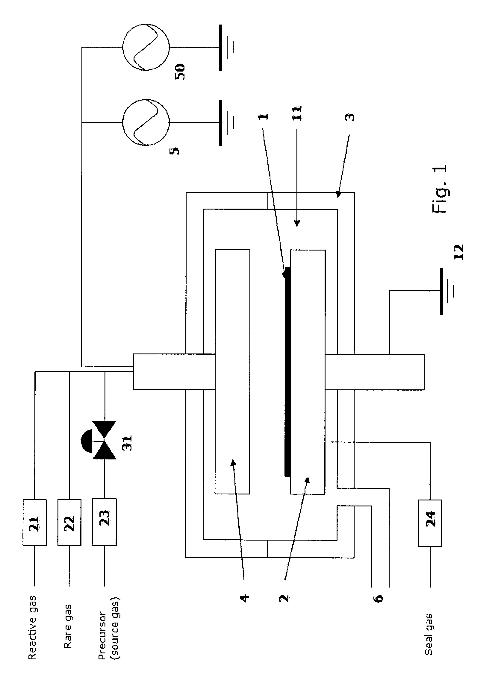
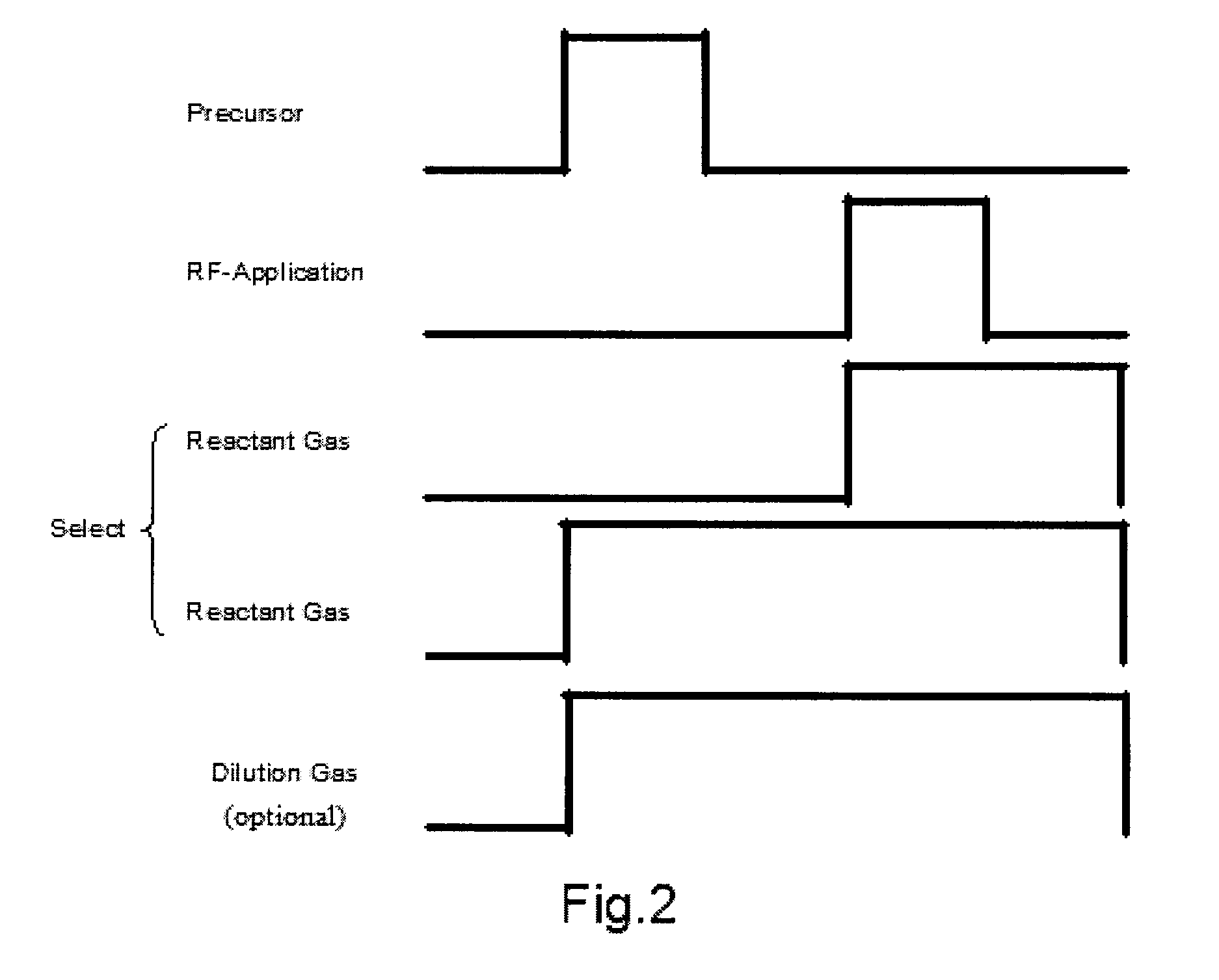
[0093]A dielectric film was formed on a 300-mm substrate having a patterned surface having an aspect ratio of about 2 and an opening width of about 50 nm under the condition shown below using Sequences 1 to 3 illustrated in FIGS. 2 to 4 and the PE-ALD apparatus illustrated in FIG. 1. The thickness of film was 30 nm for evaluating film properties.

[0094]Sequence 1:

[0095]Precursor inflow pressure: 133-1333 Pa (It depended on vapor pressure of precursor)

[0096]Carrier gas (Ar) flow: 2000 sccm

[0097]Reactant gas flow: 2000 sccm

[0098]Purge gas: He

[0099]Purge gas flow (continuous): 500 sccm

[0100]RF frequency: 13.56 MHz

[0101]Precursor supply time: 0.1-1 sec supply (It depended on vapor pressure of precursor)

[0102]Purge time: 1 sec

[0103]Reactant gas supply time (continuous): 2000 sccm

[0104]Purge time: 1 sec

[0105]RF Plasma exciting time: 1 or 3 (longer time for SiN) sec excite

[0106]Sequence 2

[0107]Same as in Sequence 1 except:

[0108]Purge time between reactant gas A pulse and reactant gas B puls...


PUM

PropertyMeasurementUnit
temperatureaaaaaaaaaa
frequencyaaaaaaaaaa
aspect ratioaaaaaaaaaa

Abstract

A method of forming a dielectric film having at least Si—N, Si—C, or Si—B bonds on a semiconductor substrate by atomic layer deposition (ALD), includes: adsorbing a precursor on a surface of a substrate; supplying a reactant gas over the surface; reacting the precursor and the reactant gas on the surface; and repeating the above steps to form a dielectric film having at least Si—N, Si—C, or Si—B bonds on the substrate. The precursor has at least one Si—C or Si—N bond, at least one hydrocarbon, and at least one halogen attached to silicon in its molecule.

Description

BACKGROUND[0001]1. Field of the Invention[0002]The present invention relates generally to semiconductor integrated circuit manufacturing and, more particularly to a method of forming a dielectric film having at least Si—N, Si—C, or Si—B bonds on a semiconductor substrate by atomic layer deposition (ALD).[0003]2. Description of the Related Art[0004]SiC, SiCN, SiCO and other silicon carbide insulation films were adopted as etching stopper films and Cu diffusion blocking films for devices installed with Cu wirings. These films provided advantages in that their film characteristics could be changed by controlling the ratios of carbon, nitrogen and oxygen and that these films offered insulation resistance despite being thin and also allowed for control of dielectric constant at low levels. Those skilled in the art have been forming these silicon carbide films using plasma CVD, where the step covering property (coverage) with these films formed on semiconductor circuits having irregular s...

Claims


Application Information

Patent Timeline
Patent Type & Authority Patents(United States)
IPC IPC(8): H01L21/00
CPCC23C16/30C23C16/45553H01L21/02167H01L21/0217H01L21/02211H01L21/02274H01L21/0228
Inventor FUKAZAWA, ATSUKITAKAMURE, NOBORU
Owner ASM JAPAN
Why Eureka
Try Eureka