
Optical modulator with three-dimensional waveguide tapers

a technology of optical modulators and waveguides, applied in the field of optical modulator circuits, can solve the problems of difficult integration of light modulators with silicon-based optical waveguides, difficult use of light modulators, and complex construction of efficient light modulators. achieve the effect of reducing optical coupling loss

Active Publication Date: 2013-03-19
ORACLE INT CORP +1
View PDF9 Cites 6 Cited by
  • Summary
  • Abstract
  • Description
  • Claims
  • Application Information

AI Technical Summary

Benefits of technology

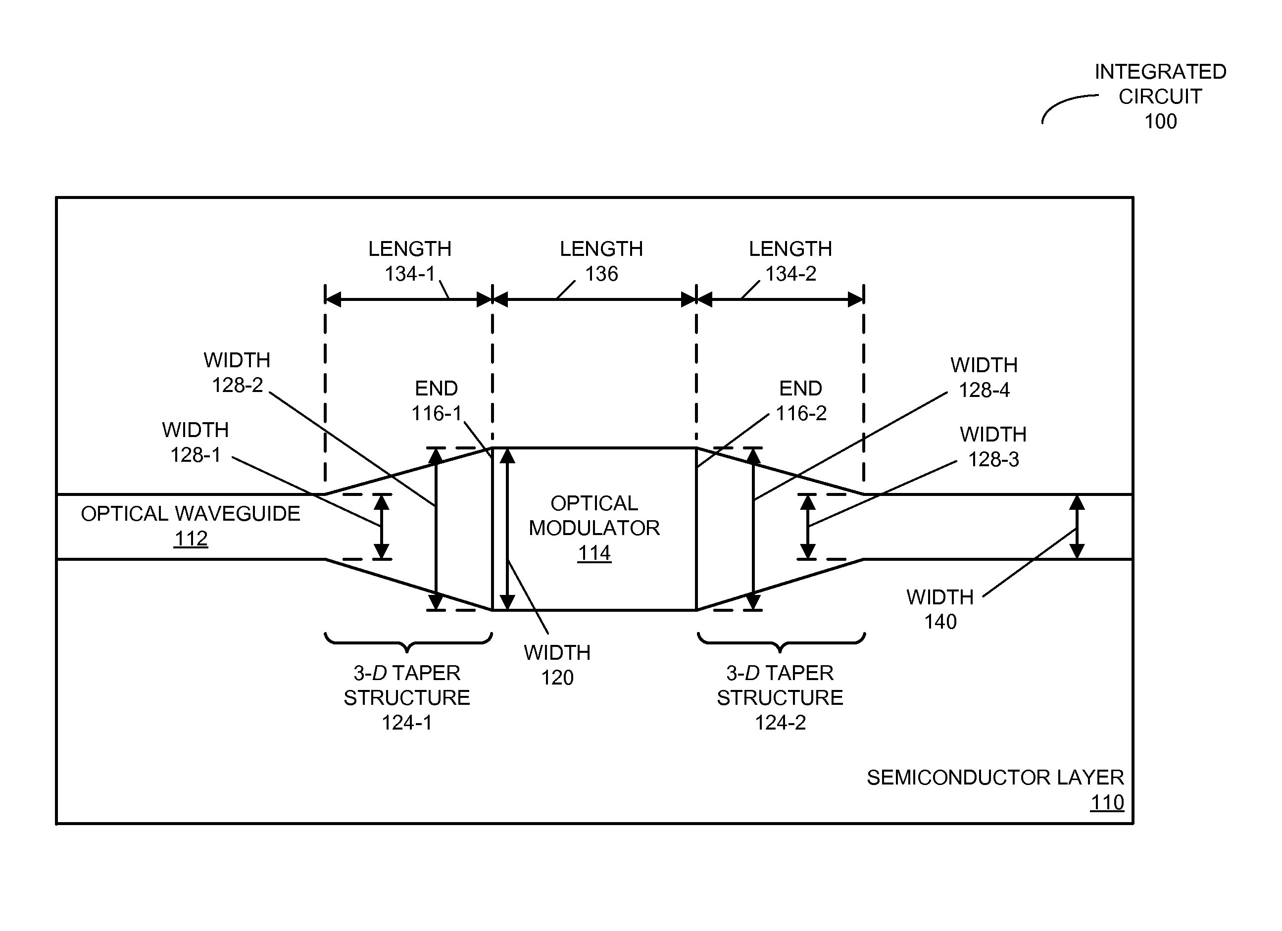
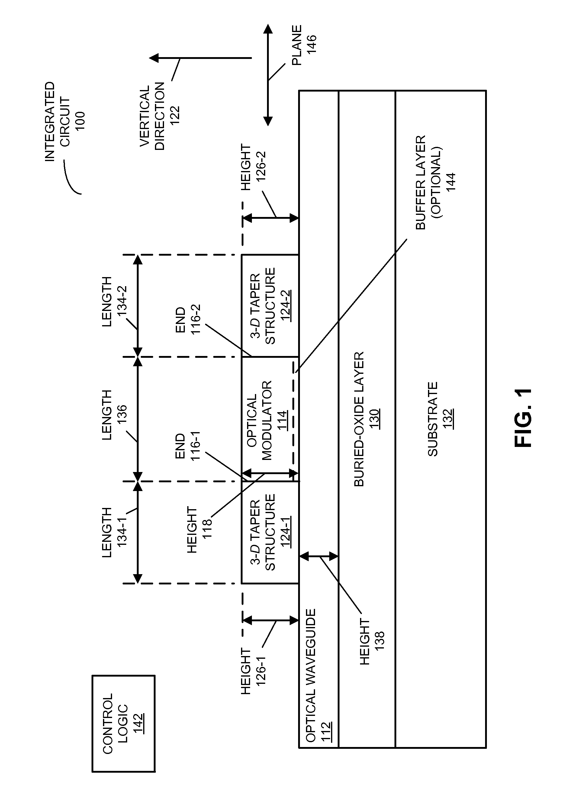
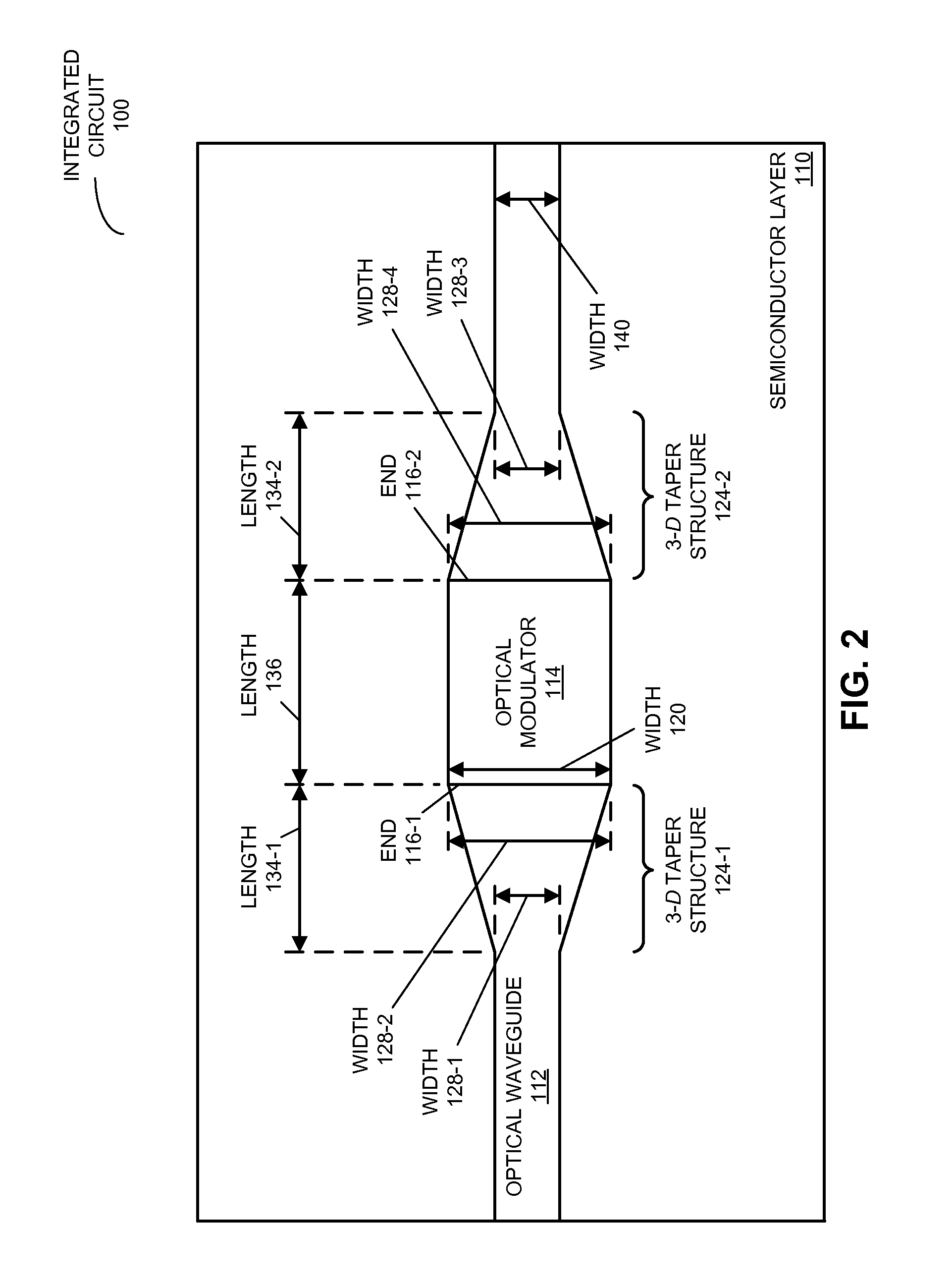
The present patent provides an integrated circuit that includes an optical waveguide and an optical modulator. A 3-D taper structure is disposed on the optical waveguide to reduce optical-coupling loss and optically modulate the optical signal. The height and cross-sectional area of the 3-D taper structure match that of the optical modulator. This results in efficient coupling of the optical signal to the optical modulator and selective optical modulation based on the modulation signal. The technical effect is improved performance and efficiency of integrated optical circuits.

Problems solved by technology

Note that it is complicated to construct efficient light modulators because the electro-optic effect in silicon (Si) is weak.
However, it is very challenging to integrate these light modulators with silicon-based optical waveguides, which makes it hard to use these light modulators.
In particular, it is very challenging to fabricate electro-absorption light modulators with sub-micron on-chip silicon optical waveguides, because epitaxial growth is needed for the active material layers in the electro-absorption light modulators, such as the multilayer QW structures or the tensile-strained germanium layer.
Moreover, it is difficult to couple the light from a sub-micron silicon optical waveguide to the active material layers to modulate the light, and then to couple the modulated light back to a sub-micron output silicon optical waveguide with low optical loss.

Method used


Image

  • Optical modulator with three-dimensional waveguide tapers
  • Optical modulator with three-dimensional waveguide tapers
  • Optical modulator with three-dimensional waveguide tapers

Examples


Embodiment Construction

[0023]Embodiments of an integrated circuit, a system that includes the integrated circuit, and a method for selectively optically modulating an optical signal in the integrated circuit are described. This integrated circuit includes an optical waveguide defined in a semiconductor layer. Furthermore, light is coupled between the optical waveguide and an optical modulator, which is disposed on the optical waveguide, using 3-dimensional (3-D) taper structures that are proximate to the ends of the optical modulator. The cross-sectional areas of these 3-D taper structures transition, over a distance, from that of the optical waveguide (distal from the optical modulator) to that of optical modulator (proximate to the ends of the optical modulator). In this way, a spatial extent of an optical mode in the optical waveguide and a spatial extent of an optical mode in the optical modulator may be approximately matched to reduce the optical loss when light is coupled to or from the optical modu...


PUM

PropertyMeasurementUnit
optical-mode sizeaaaaaaaaaa
lengthsaaaaaaaaaa

Abstract

An integrated circuit that includes an optical waveguide defined in a semiconductor layer is described. In this integrated circuit, light is coupled between the optical waveguide and an optical modulator, which is disposed on the optical waveguide, using 3-dimensional (3-D) taper structures that are proximate to the ends of the optical modulator. The cross-sectional areas of these 3-D taper structures transition, over a distance, from that of the optical waveguide (distal from the optical modulator) to that of optical modulator (proximate to the ends of the optical modulator). In this way, a spatial extent of an optical mode in the optical waveguide and a spatial extent of the optical mode in the optical modulator may be approximately matched to reduce the optical loss when the light is coupled to or from the optical modulator.

Description

GOVERNMENT LICENSE RIGHTS[0001]The United States Government has a paid-up license in this invention and the right in limited circumstances to require the patent owner to license others on reasonable terms as provided for by the terms of Agreement No. HR0011-08-9-0001 awarded by the Defense Advanced Research Projects Administration.BACKGROUND[0002]1. Field[0003]The present disclosure generally relates to optical-modulator circuits. More specifically, the present disclosure relates to an optical-modulator circuit that includes three-dimensional waveguide tapers.[0004]2. Related Art[0005]Silicon photonics is a promising new technology that can potentially provide low-power, high-bandwidth and low-latency interconnects in future computing systems. However, in order to implement practical silicon photonic links, efficient light modulators are needed. Note that it is complicated to construct efficient light modulators because the electro-optic effect in silicon (Si) is weak. As a conseque...

Claims


Application Information

Patent Timeline
Patent Type & Authority Patents(United States)
IPC IPC(8): G02F1/035
CPCG02B6/1228G02F2001/0157G02F1/01708G02F1/0157
Inventor ZHENG, XUEZHECUNNINGHAM, JOHN E.KRISHNAMOORTHY, ASHOK V.FENG, DAZENGASGHARI, MEHDI
Owner ORACLE INT CORP
Learn More