
Frame interconnect for concentrated photovoltaic module

a photovoltaic module and interconnect technology, applied in the field of semiconductor devices, can solve the problems of reducing the overall utility of the device, difficult to control the shape and the shape control of the ribbon/mesh type interconnect for automatic pick-up is not good, so as to reduce optical coupling loss, increase the rigidity of the structure, and increase placement accuracy

Active Publication Date: 2014-10-21
AMKOR TECH SINGAPORE HLDG PTE LTD
View PDF22 Cites 1 Cited by
  • Summary
  • Abstract
  • Description
  • Claims
  • Application Information

AI Technical Summary

Benefits of technology

The present invention provides various embodiments of a CPV module with a frame interconnect that allows for a high current carrying capacity, continuous contact with the bus bar, and no current crowding. The fabrication process of the module is compatible with standard automated assembly equipment, and requires no encapsulation. The frame interconnect includes integrated features for aligning a glass prism or optical light guide, and may also include an integrated electrical contact and / or cable connector. The frame interconnect also forms a light shield around the receiver die to protect other components from intense solar energy damage. The fourth embodiment of the invention includes an added folded cable connector on one side to capture the exposed end of an insulated cable which forms an electrical connection with the CPV module. The fifth embodiment includes an invention where the frame interconnect has one section of an upward tab shaped and bent downward to form electrical contact with a bypass diode mounted on the substrate of the CPV module. The bent metal sheet also provides better current carrying capability and reliability against harsh environments.

Problems solved by technology

However, the use of the ribbon / mesh type interconnects or, alternatively, the wire bonds give rise to certain deficiencies in currently known CPV modules which detract from their overall utility.
More particularly, the ribbon / mesh type interconnects do not have good shape control for automatic pick up, and require the use of specialized welding equipment for the fabrication of the CPV module using the same.
Stated another way, it is often difficult to control the shape of the ribbon / mesh type interconnects for automatic pick up and placement, with the fabrication process being mostly done through the use of special welding equipment or manual soldering which is more labor intensive and thus more costly.
In addition, in those CPV modules including bond wires, problems may arise in relation to current crowding if too few wires are used.
Moreover, the use of the soldered or welded ribbon / mesh interconnects or bond wires creates concerns regarding the electrical current carrying capability of the CPV module including the same.

Method used


Image

  • Frame interconnect for concentrated photovoltaic module
  • Frame interconnect for concentrated photovoltaic module
  • Frame interconnect for concentrated photovoltaic module

Examples


first embodiment

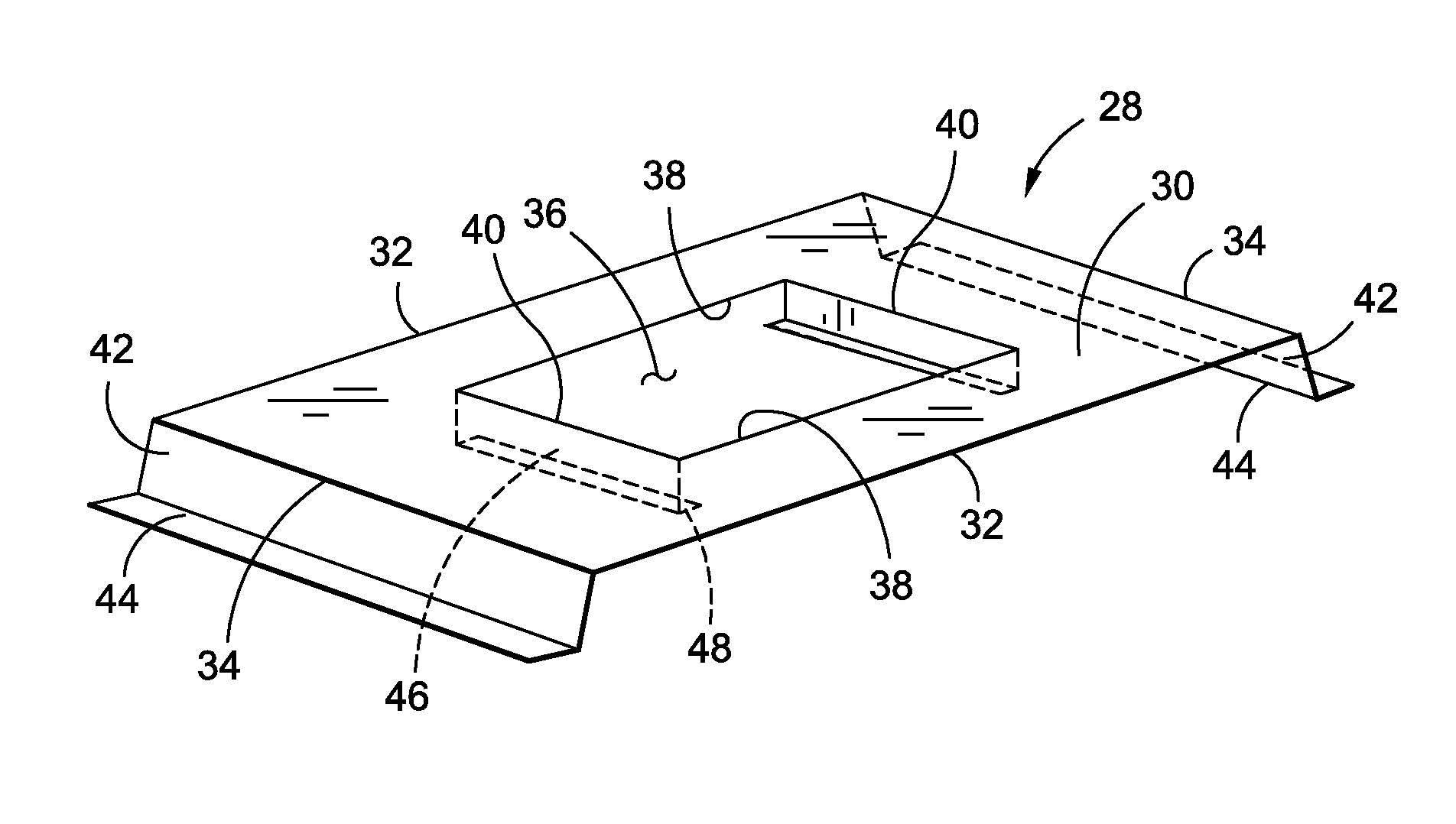
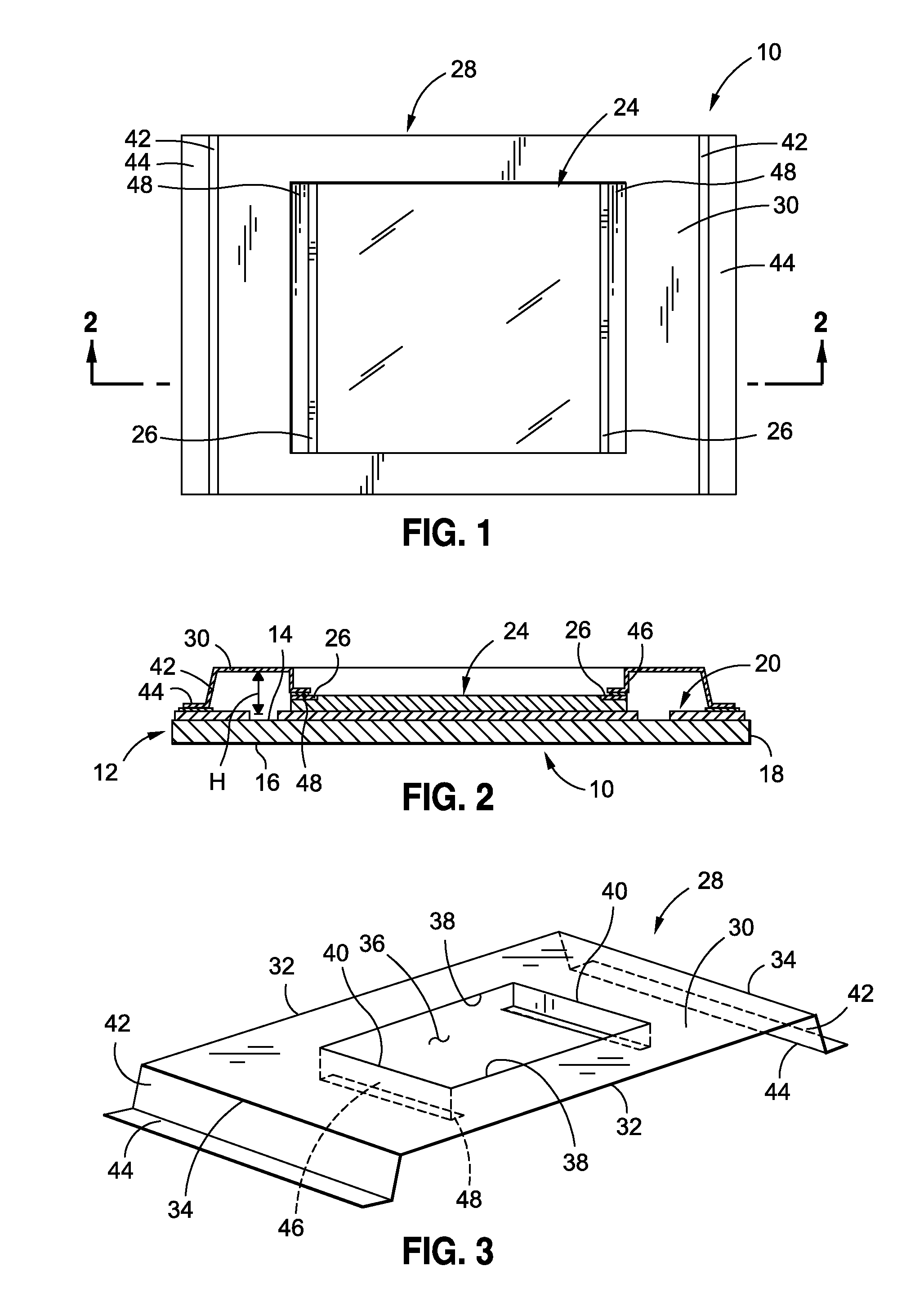
[0031]Referring now to the drawings wherein the showings are for purposes of illustrating preferred embodiments of the present invention only, and not for purposes of limiting the same, FIGS. 1-3 depict a CPV module 10 constructed in accordance with the present invention. The module 10 comprises a substrate 12 which has a generally quadrangular (e.g., rectangular, square) configuration. When viewed from the perspective shown in FIG. 2, the substrate 12 defines a generally planar top surface 14, and an opposed, generally planar bottom surface 16. Extending generally perpendicularly between the top and bottom surfaces 14, 16 is a peripheral side surface 18 of the substrate 12. Disposed on the top surface 14 of the substrate 12 is an electrically conductive pattern 20 which may be formed in any one of a multiplicity of different configurations or arrangements on the top surface 14.

[0032]The module 10 constructed in accordance with the present invention further comprises a receiver die ...

second embodiment

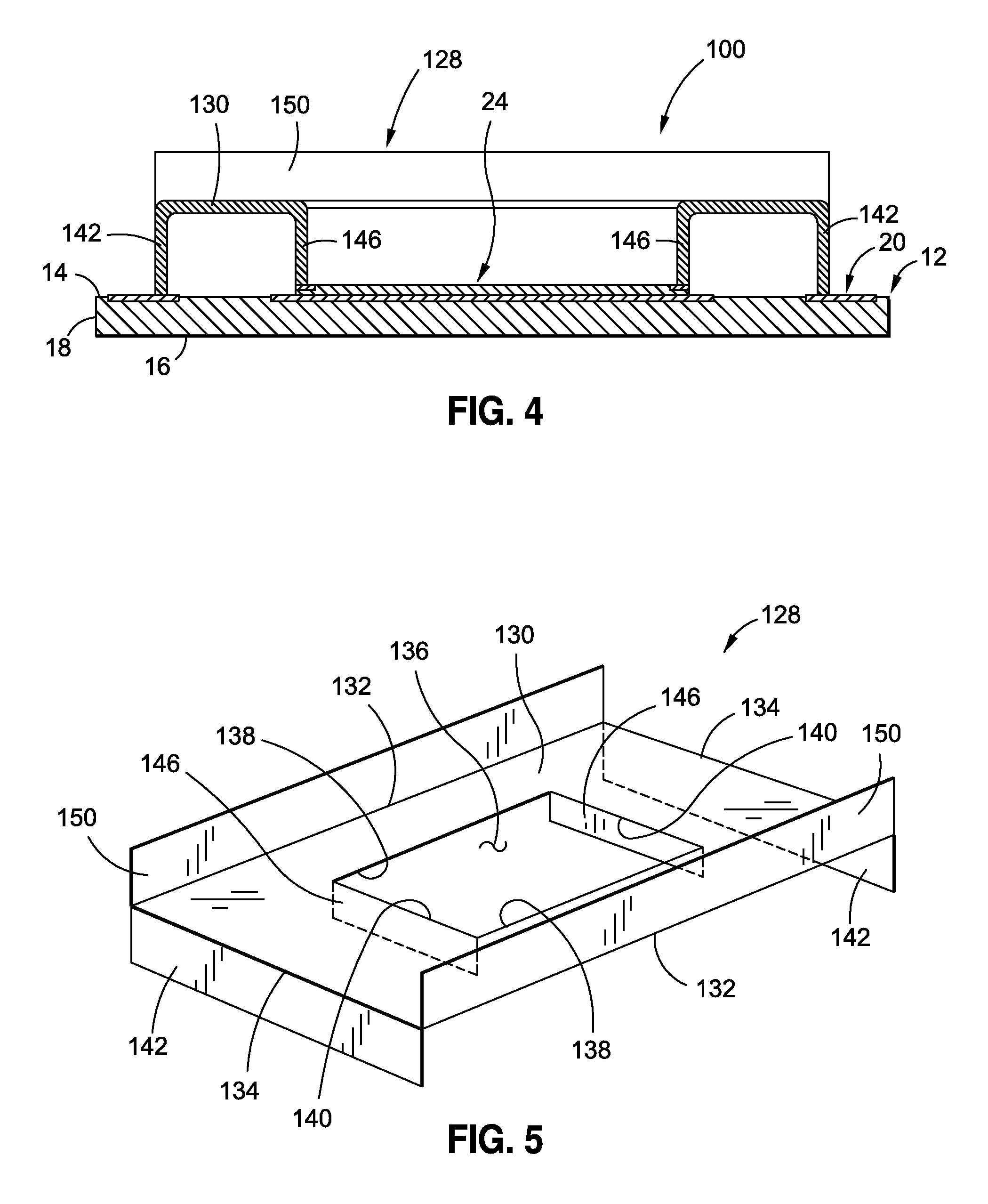
[0042]Referring now to FIG. 4, there is shown in cross-section a CPV module 100 constructed in accordance with the present invention. The module 100 is similar in structure to the above-described module 10, with only the distinctions between the modules 100, 10 being described below.

[0043]The sole distinction between the CPV modules 100, 10 lies in the structural attributes of the frame interconnect 128 included in the module 100, in comparison to the frame interconnect 28 of the module 10. In the module 100, the frame interconnect 128 is fabricated from a single metal sheet with a solderable finish which is bent to define various structural features. In particular, the frame interconnect 128 is formed to define a generally planar main body portion 130 which has a generally quadrangular configuration. As shown in FIGS. 4 and 5, the main body portion 130 has a generally rectangular configuration defining an opposed, generally parallel pair of outer longitudinal sides 132, and an oppo...

third embodiment

[0050]Referring now to FIG. 6, there is shown in cross-section a CPV module 200 constructed in accordance with the present invention. The module 200 is substantially similar in structure to the above-described module 100, with the sole distinction between the CPV modules 200, 100 lying in the inclusion of a slight structural modification in the frame interconnect 228 included in the module 200, in comparison to the frame interconnect 128 of the module 100. In this regard, only the structural differences between the frame interconnects 228, 128 will be described below. The frame interconnect 228 is shown in FIG. 7 separate from the module 200.

[0051]More particularly, in the frame interconnect 228, each adjacent pair of inner longitudinal and lateral sides 138, 140 is separated from each other by a chamfered corner 252. Thus, in the frame interconnect 228 included in the module 200, the window 136 thereof is collectively defined by the inner longitudinal and lateral sides 138, 140 and...


PUM


Abstract

In accordance with the present invention, there is provided multiple embodiments of a concentrated photovoltaic (CPV) receiver package or module which includes a uniquely configured frame interconnect to facilitate the electrical connection of a receiver die of the CPV module to the conductive pattern of an underlying substrate thereof. In each embodiment of the present invention, a single piece of sheet metal is bent to form features to fit over the bus bar on the receiver die and bond pads of the conductive pattern on the substrate. Electrical connections can be made by soldering or conductive paste attach. Elevated, flat areas between connections facilitates vacuum pick up and automatic assembly and provides high potential insulation between connects. Additionally, in each embodiment of the present invention, the piece of bent sheet metal used to form the frame interconnect of the CPV module includes a solderable surface finish, and defines a window to accommodate an optical prism or other light guide for concentrating solar rays.

Description

CROSS-REFERENCE TO RELATED APPLICATIONS[0001]Not ApplicableSTATEMENT RE: FEDERALLY SPONSORED RESEARCH / DEVELOPMENT[0002]Not ApplicableBACKGROUND OF THE INVENTION[0003]1. Technical Field of the Invention[0004]The present invention relates generally to semiconductor devices, and more particularly to a robust, cost effective frame interconnect structure suitable for a concentrated photovoltaic (CPV) receiver module.[0005]2. Description of the Related Art[0006]Photovoltaic cells are a well known means for producing electrical current from electromagnetic radiation. Traditional photovoltaic cells comprise junction diodes fabricated from appropriately doped semiconductor materials. Such devices are typically fabricated as thin, flat wafers with the junction formed parallel to and near one of the flat surfaces. Photovoltaic cells are intended to be illuminated through their so-called “front” surface. Electromagnetic radiation absorbed by the semiconductor produces electron-hole pairs in the...

Claims


Application Information

Patent Timeline
Patent Type & Authority Patents(United States)
IPC IPC(8): H01L31/042H01L31/00
CPCH01L31/042H01L31/00Y02E10/52H01L31/02008Y02E10/50
Inventor KUO, BOB SHIH-WEIPARK, SUNGSUN
Owner AMKOR TECH SINGAPORE HLDG PTE LTD
Learn More