Optical module

a technology of optical modules and optical couplings, applied in the field of optical modules, can solve the problems of reducing cost, increasing assembling process, optical loss, etc., and achieve the effects of reducing the width or thickness of the waveguide, reducing the loss of optical coupling, and high-efficiency optical coupling

Inactive Publication Date: 2005-08-30
NEC CORP
View PDF23 Cites 5 Cited by
  • Summary
  • Abstract
  • Description
  • Claims
  • Application Information

AI Technical Summary

Benefits of technology

[0035]It is apparent from the above-mentioned equation (1) that, so as to reduce the optical coupling loss between two optical waveguides, the spot-sizes of light that is guided by both the optical waveguides should be caused to accord (refer to Kenji Kouno, “Basis And Application of Optical Coupling Systems For Optical Devices” (Gendai Kougakusya)).
[0036]The photoreceptive angle of the optical waveguide is inversely proportional to the spot-size. Namely, the photoreceptive angle (also an angle of divergence of light being emitted) increases when the spot-size is reduced, and to the contrary, the photoreceptive angle (also an angle of divergence of light being emitted) reduces when the spot-size is increased. In the present invention, the highly efficient optical coupling between the optical active element and the waveguide is accomplished by utilizing it.
[0037]In the spot-size conversion region that is configured by reducing a width or a thickness of the waveguide, or both thereof all the more in the light-emitting element side, the spot-size of the optical waveguide comes to be reduced, whereby, for example, a large angle of divergence of the LD can be converted into a small photoreceptive angle of the optical waveguide.
[0038]In the spot-size conversion region that is configured by increasing a width or a thickness of the waveguide, or both thereof all the more in the photoreceptive element side, the spot-size of the optical waveguide comes to be expanded, whereby an angle of divergence of light being emitted from the optical waveguide becomes small and, as a result, efficiency of light incident on the photoreceptive element becomes high.
[0039]Since the spot-size conversion region described above is a part of a waveguide structure, it can be built therein together with the optical waveguide, thereby not incurring an increase in the manufacturing process.

Problems solved by technology

In general, as to the optical fiber and the optical waveguide, a photoreceptive angle at which incident light is guided has been determined, and light that entered beyond its photoreceptive angle is not guided, resulting in an optical loss.
Additionally, it was proposed that, by using a micro optical system such as a lens and a tip-ball fiber (one having the tip section of the optical fiber processed in a sphere) to convert a large angle of divergence of the LD into a small photoreceptive angle of the optical waveguide, optical coupling efficiency between the LD and the waveguide was enhanced; however, in this case, parts such as the lens increase, and simultaneously, assembling process increases, whereby the problem occurs in terms of the cost reduction.

Method used


Image

  • Optical module
  • Optical module
  • Optical module

Examples


embodiment 1

(Embodiment 1)

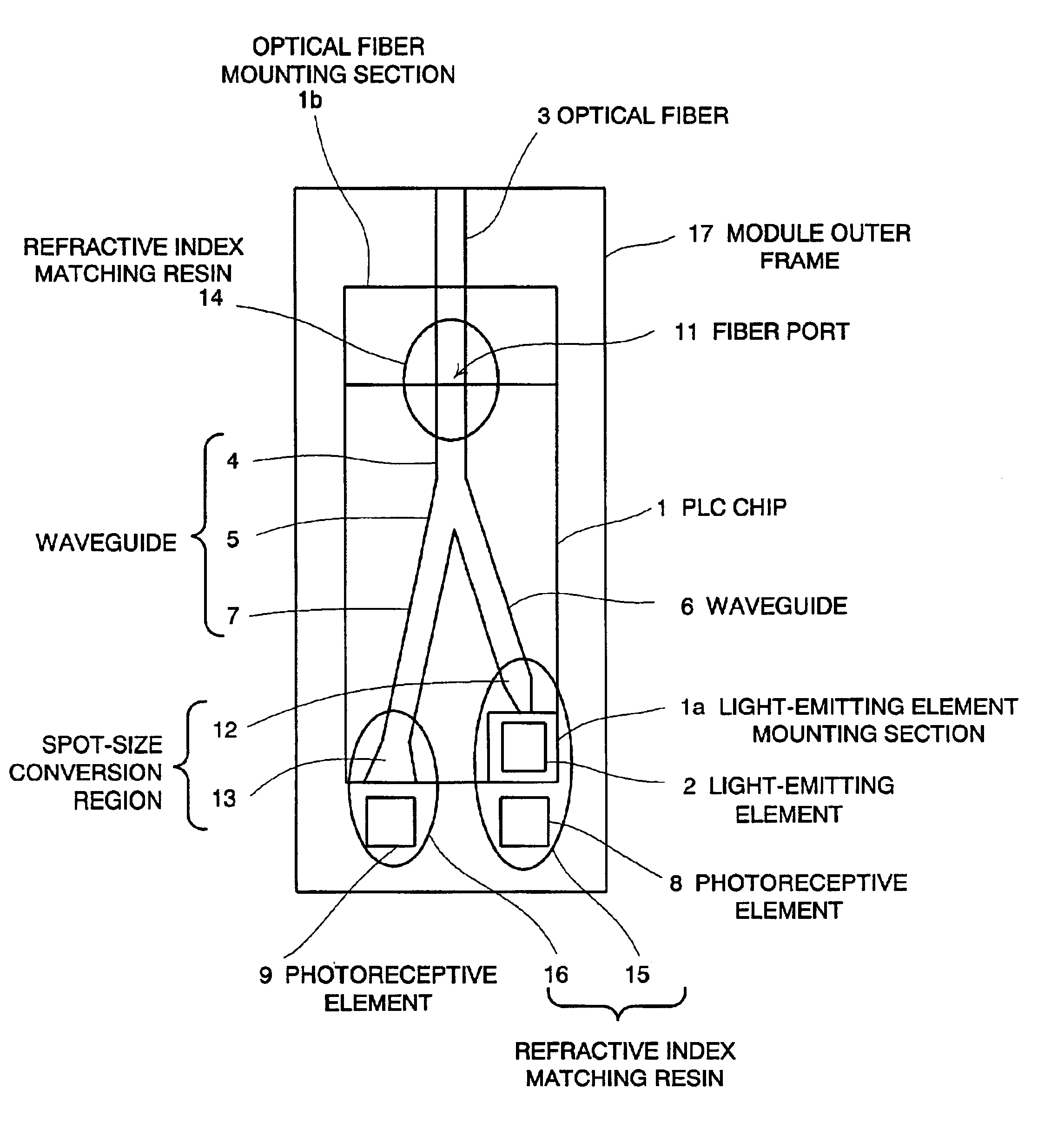
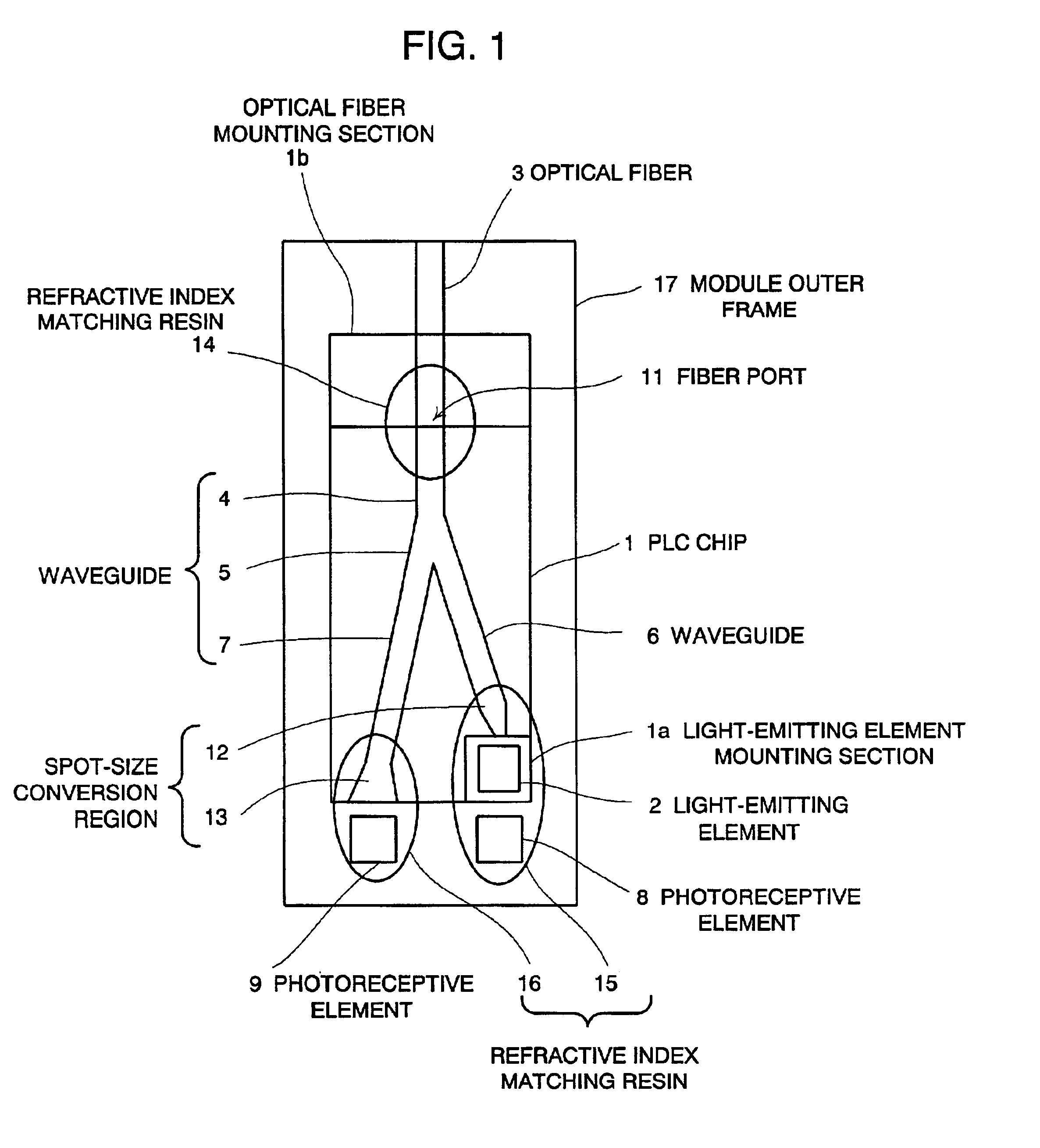
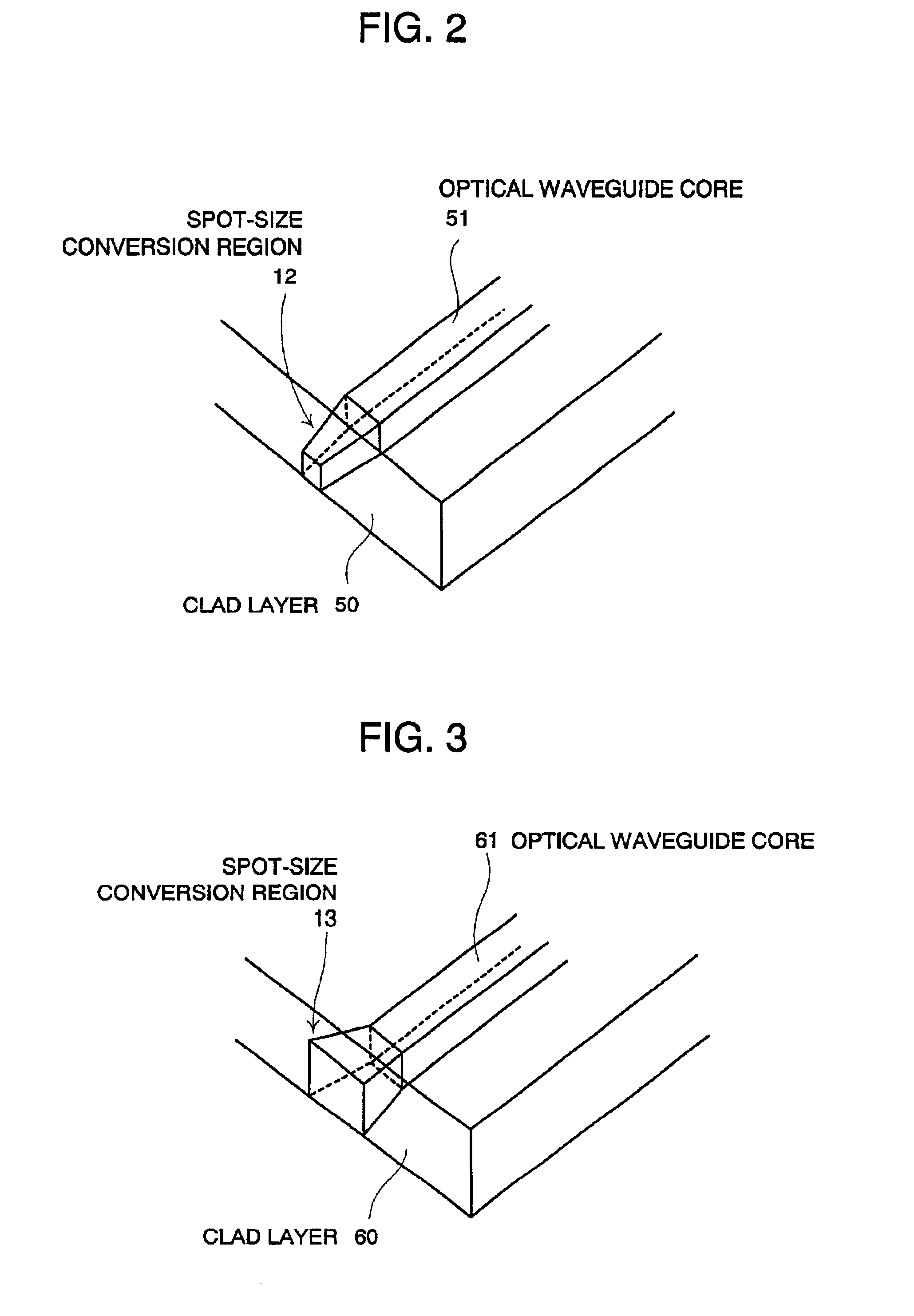
[0052]FIG. 1 is a top plan view illustrating a schematic configuration of an optical transmitter / receiver module that is a first embodiment of the present invention. This optical transmitter / receiver module has a structure in which: a PLC chip 1 in which waveguides 4 to 7, a light-emitting element mounting section 1a and an optical fiber mounting section 1b were formed; a light-emitting element 2 such as the LD mounted on the light-emitting element mounting section 1a on the PLC chip 1; an optical fiber 3 that introduces the send light outside the module or introduces the receive light from the exterior within the module, which was mounted on the optical fiber mounting section 1b on the PLC chip 1; and photoreceptive elements 8 and 9 such as the PD were provided on a substrate and were contained within a module outer frame 17.

[0053]The waveguides 4 to 7 configure the waveguide having a symmetric Y-type branch structure as a whole. Namely, this symmetric Y-type branch w...

embodiment 2

(Embodiment 2)

[0082]FIG. 9 is a top plan view illustrating a schematic configuration of an optical transmitter / receiver module that is a second embodiment of the present invention. This optical transmitter / receiver module is a module having a wavelength division multiplex structure in which a layout of the optical active element and the optical waveguide of the structure of the foregoing first embodiment was changed to provide a WDM (Wavelength Division Multiplex) filter 31. The effect accompanying the spot-size conversion explained in the foregoing first embodiment is also similarly obtained in this embodiment; however, herein, for simplification of explanation, its explanation is omitted for convenience and only the different part from the first embodiment will be explained.

[0083]On a substrate are provided and within a module outer frame 37 are contained: a PLC chip 21 in which waveguides 24 to 27, a light-emitting element mounting section 21a and an optical fiber mounting sectio...


PUM


Abstract

An optical module includes a waveguide. In one aspect, an optical active element and an optical waveguide are formed separately, with the optical waveguide being optically coupled to the optical active element, and with the optical waveguide including a spot-size conversion region. In another aspect, a refractive index matching resin, having the same-level refractive index as that of the optical waveguide, is provided between the waveguide and the optical active element. In a further aspect, the waveguide is a Y-type branch waveguide in which a single-mode waveguide section is branched into first and second branch waveguide sections. In a yet another aspect, a device which divides lights of different wavelengths is provided to reflect light of a first wavelength and pass light of another wavelength, separating incoming light from outgoing light.

Description

BACKGROUND OF THE INVENTION[0001]The present invention relates to an optical module for use in an optical communication system.[0002]Recently, development of an optical module using a PLC (Planar Lightwave Circuit), which has a laser diode (LD), a photo diode (PD) and electric elements integrated, has progressed in an optical communication system. For example, in the Electronics Society Meeting C-3-6, 1997, of the Electronic Information Communication Society and in JP-A-191152 / 1997 were proposed an optical module having a light-emitting element (the LD and so forth) and a photoreceptive element (the PD and so forth) mounted on a waveguide substrate.[0003]FIG. 10 is a perspective view illustrating a schematic configuration of the optical module disclosed in the above-mentioned documents. This optical module is a module having a light-emitting element 102 and photoreceptive elements 108 and 109 mounted on a waveguide substrate 101 in which waveguides 104 to 107 were formed. The wavegu...

Claims


Application Information

Patent Timeline
Patent Type & Authority Patents(United States)
IPC IPC(8): G02B6/12G02B6/125G02B6/122G02B6/42G02B6/30H01L31/0232H01L33/48H01S5/022
CPCG02B6/12004G02B6/1228G02B6/125G02B6/4212G02B6/42G02B6/4246
Inventor OGURO, MAMORU
Owner NEC CORP
Why Eureka
Try Eureka