Electro-optic modulator

a technology of optical modulator and optical modulator, which is applied in the field of optical modulator, can solve the problems of low modulation efficiency, limited use of such devices, and modulation length, and achieve the effects of improving modulation efficiency, high optical coupling efficiency, and reducing electric capacity and lead-out resistan

Active Publication Date: 2021-05-04
NEC CORP +1
View PDF10 Cites 3 Cited by
  • Summary
  • Abstract
  • Description
  • Claims
  • Application Information

AI Technical Summary

Benefits of technology

[0010]It is an object of the present invention to provide a SIS-type electro-optic modulator capable of realizing highly efficient optical coupling with a rib-type Si waveguide, improving modulation efficiency, realizing reduction of electric capacity and lead-out resistance in stacked semiconductor layers.
[0012]According to one aspect of the present invention, it is possible to provide an SIS type electro-optic modulator capable of realizing highly efficient optical coupling with a rib-type Si waveguide, improving modulation efficiency, realizing reduction of electric capacity and lead-out resistance in stacked semiconductor layers, and capable of integration on the Si substrate.

Problems solved by technology

However, optical switches and optical modulators that use a thermo-optic effect of silicon to change the refractive index operate at low speed, and accordingly their use is limited to cases of device speeds corresponding to modulation frequencies not higher than 1 Mb / second.
Most of such devices that have been studied to date have low optical modulation efficiency, and accordingly, for optical phase modulation, require a length on the order of millimeters and an injection current density higher than 1 kA / cm3.
If the device size is large, the device becomes susceptible to the influence of temperature distribution over the silicon platform, and it is therefore assumed that a change in the refractive index of the silicon layer caused by a thermo-optic effect due to the temperature distribution cancels out the essentially existing electro-optic effect, thus raising a problem.
However, in practice there is a problem in that the region where the carrier density dynamically changes is an extremely thin region with a size of about several tens of nanometers, which results in the problem that an optical modulation length on the order of millimeters is required, and the electro-optic modulator accordingly becomes large in size, and consequently high-speed operation is difficult.
On the other hand, when the electrode layer formed adjacent to the second silicon layer of the second conductivity type is brought close to the rib waveguide, the optical loss becomes large.
Therefore, with regard to the SIS-type electro-optic modulator that can be downsized and lowered in voltage, it is an issue to improve the modulation efficiency and reduce the power consumption and the frequency band by reducing the electric capacity.

Method used


Image

  • Electro-optic modulator
  • Electro-optic modulator
  • Electro-optic modulator

Examples


Embodiment Construction

[0025]Hereinafter, the present invention will be described with example embodiments.

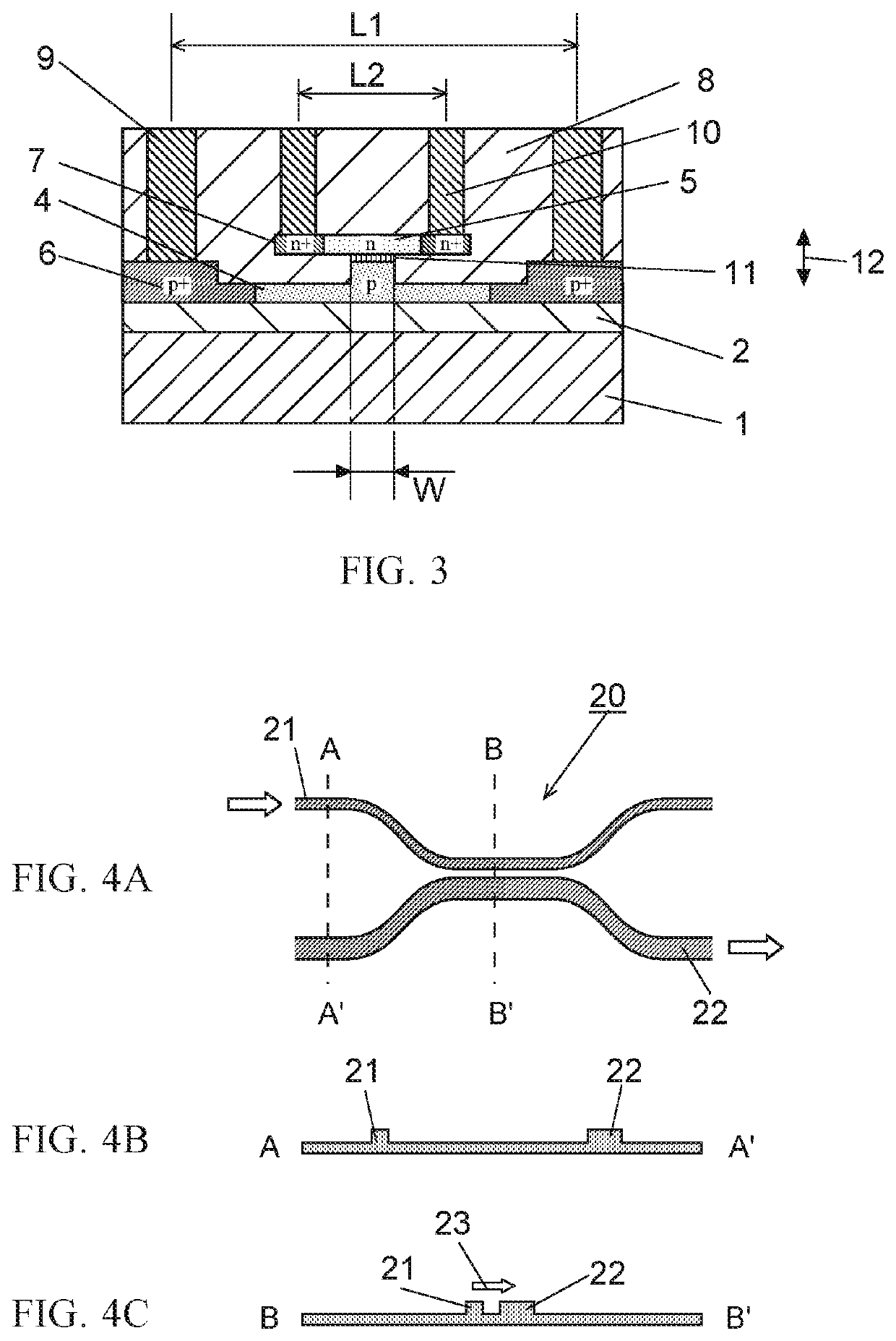
[0026]FIG. 3 is a cross-sectional view of an electro-optic modulator including an SIS structure according to one example embodiment of the present invention. Here, the first conductivity type is described as p-type and the second conductivity type is described as n-type, but conversely, the first conductivity type may be n-type and the second conductivity type may be p-type.

[0027]In FIG. 3, a first semiconductor layer 4 doped to exhibit a first type of conductivity (p-type conductivity) and a second semiconductor layer 5 doped to exhibit a second type of conductivity (n-type conductivity) are disposed parallel to support substrate 1 of an SOI substrate via buried oxide (BOX) layer 2 which constitutes a lower clad, and both semiconductor layers are at least partially stacked. Between the stacked semiconductor layers, a dielectric layer 11 is disposed to form SIS type junction. In FIG. 3, the first sem...


PUM

PropertyMeasurementUnit
wavelengthsaaaaaaaaaa
thicknessaaaaaaaaaa

Abstract

Provided is a SIS-type electro-optic modulator capable of realizing highly efficient optical coupling with a rib-type Si waveguide, improving modulation efficiency, realizing reduction of electric capacity and lead-out resistance in stacked semiconductor layers. The modulator includes a SIS junction constituted by first and second semiconductor layers having different type of conductivity and a dielectric layer interposed therebetween, wherein an electrical signal from electrodes coupled to the first and second semiconductor layers causes free carriers accumulate, deplete or invert on both sides of the dielectric layer, thereby modulating a free carrier concentration felt by an optical signal electric filed, light having a polarization component orthogonal to the width direction of the SIS junction is incident on the dielectric layer, and the width of the SIS junction is λ / neff or less (λ is the wavelength of the incident light and neff is an effective refractive index of the modulator to the incident light).

Description

INCORPORATION BY REFERENCE[0001]This application is based upon and claims the benefit of priority from Japanese patent application No. 2018-113707, filed on Jun. 14, 2018, the disclosure of which is incorporated herein in its entirety by reference.TECHNICAL FIELD[0002]The present invention relates to an electro-optic modulator for high speed conversion of high speed electrical signals into optical signals that is required in the information processing and telecommunications fields.BACKGROUND ART[0003]Optical communication devices using silicon photonics and functioning at 1310 and 1550 nm fiber-optic communication wavelengths for a variety of systems such as for fiber-to-the-home and local area networks (LANs) are highly promising technologies which enable integration of optical functioning elements and electronic circuits together on a silicon platform by means of CMOS technologies.[0004]In recent years, silicon-based passive optical devices such as waveguides, couplers and wavelen...

Claims


Application Information

Patent Timeline
Patent Type & Authority Patents(United States)
IPC IPC(8): G02F1/225G02F1/21
CPCG02F1/2257G02F2001/212G02F2201/063G02F1/212
Inventor TAKAHASHI, SHIGEKIFUJIKATA, JUNICHI
Owner NEC CORP
Why Eureka
Try Eureka