Method for forming semiconductor thin film and method for manufacturing thin-film semiconductor device

a technology of semiconductors and thin films, applied in the direction of solid-state devices, basic electric elements, thermoelectric devices, etc., can solve the problems of mobility degradation by heating, and achieve the suppression of mobility deterioration, the effect of preventing characteristic deterioration due to heating and suppressing mobility

Inactive Publication Date: 2013-04-09
SONY CORP
View PDF5 Cites 4 Cited by
  • Summary
  • Abstract
  • Description
  • Claims
  • Application Information

AI Technical Summary

Benefits of technology

[0008]As described above, according to the present invention, in a semiconductor thin film and a thin-film semiconductor device using the thin film, a layered structure semiconductor thin film capable of suppressing decrease in mobility due to heating and characteristic deterioration due to the decrease in mobility can be obtained according to very simple procedures.

Problems solved by technology

However, thin-film semiconductor devices using organic semiconductor thin films have the problem that mobility is degraded by heating.

Method used


Image

  • Method for forming semiconductor thin film and method for manufacturing thin-film semiconductor device
  • Method for forming semiconductor thin film and method for manufacturing thin-film semiconductor device
  • Method for forming semiconductor thin film and method for manufacturing thin-film semiconductor device

Examples


examples

Preparation of Semiconductor Thin Film-1

Poly(Alpha-Methylstyrene)

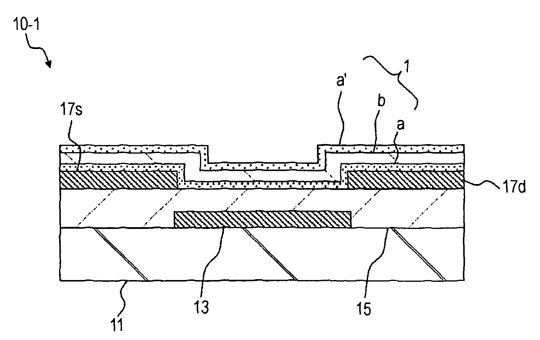
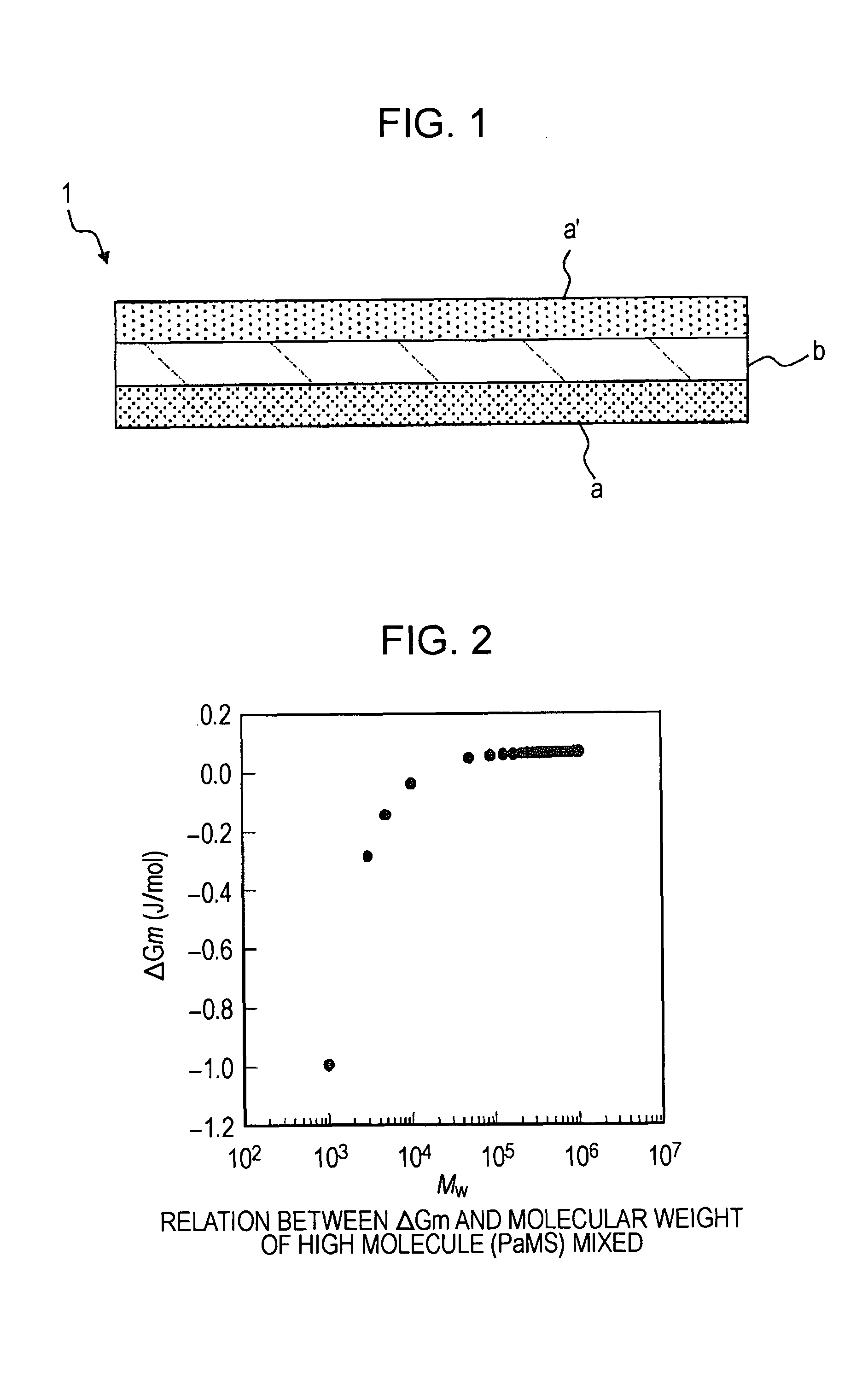
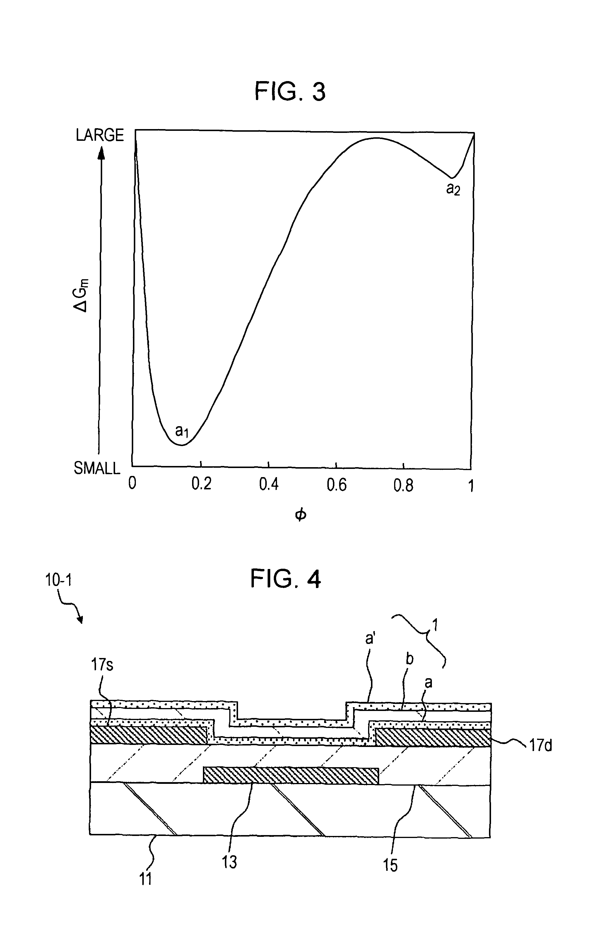
[0154]TIPS pentacene was used as an organic semiconductor material, poly(alpha-methylstyrene) (PaMS) was used a different organic material, and these materials were mixed and dissolved in mesitylene to prepare a solution. In addition, the TIPS pentacene was used as a conjugated low-molecular organic semiconductor material. Also, the PaMS was used as a high-molecular insulating material.

[0155]Here, as the PaMS which was a high-molecular insulating material, PaMS having each of the molecular weights shown in of Table 1 below was used, and the solution was prepared at a mixing ratio of TIPS pentacene:PaMS=1:1.

[0156]

TABLE 1Molecular weight of PaMSMnMwMw / Mn196022001.1227600282001.0258000591001.021060001080001.028070008680001.08

[0157]Also, as shown in Table 1, PaMS having a narrow molecular weight distribution was used, in which the values of number-average molecular weight (Mn) and weight-average molecular weight (Mw) were...


PUM

PropertyMeasurementUnit
heat-resistant temperatureaaaaaaaaaa
semiconductoraaaaaaaaaa
molecular weightaaaaaaaaaa

Abstract

The present invention provides a method for forming a semiconductor thin film, which is capable of suppressing decrease in mobility due to heating and characteristic deterioration due to the decrease in mobility and which is capable of forming a semiconductor thin film with improved heat resistance by more simple procedures. A solution in which a plurality of types of organic materials including an organic semiconductor material are mixed is applied or printed on a substrate to form a thin film, and the plurality of types of organic materials are phase-separated by a process of drying the thin film. As a result, a layered structure semiconductor thin film is obtained, in which an intermediate layer b composed of an organic insulating material is sandwiched between two semiconductor layers a and a′.

Description

TECHNICAL FIELD[0001]The present invention relates to a method for forming a semiconductor thin film, particularly a method for forming an organic semiconductor thin film which is capable of suppressing characteristic deterioration due to heating, and a method for manufacturing a thin-film semiconductor device using the forming method.BACKGROUND ART[0002]In manufacturing thin-film semiconductor devices using organic semiconductor thin films, such as organic thin-film transistors (organic TFT), the organic semiconductor thin films can be formed by applying a coating / printing process. For example, an organic semiconductor thin film composed of an organic semiconductor material with a single configuration can be obtained by coating a substrate with a solution prepared by dissolving the organic semiconductor material in a solvent and then drying the resulting coating. Therefore, attempts can be made to increase the substrate size and decrease the manufacturing cost as compared with conv...

Claims


Application Information

Patent Timeline
Patent Type & Authority Patents(United States)
IPC IPC(8): H01L51/40
CPCH01L51/0003H01L51/0562H01L51/052H10K71/12H10K10/471H10K10/486
Inventor OHE, TAKAHIROKIMIJIMA, MIKI
Owner SONY CORP
Why Eureka
Try Eureka