Silicon carbide semiconductor device

a technology of silicon carbide and semiconductors, applied in the direction of semiconductor devices, basic electric elements, electrical appliances, etc., can solve the problems of more interface traps at the mos interface and poor quality of the mos interface, and achieve the effect of reducing the decrease in channel mobility, effectively increasing the threshold voltage, and improving the trade-off relationship between channel mobility and threshold voltag

Active Publication Date: 2018-06-19
MITSUBISHI ELECTRIC CORP
View PDF15 Cites 0 Cited by
  • Summary
  • Abstract
  • Description
  • Claims
  • Application Information

AI Technical Summary

Benefits of technology

[0011]The silicon carbide semiconductor device of the present invention can suppress the decrease in the channel mobility and effectively increase the threshold voltage. In other words, the trade-off relationship between the channel mobility and the threshold voltage can be improved.

Problems solved by technology

When silicon carbide is used in comparison with silicon (Si) typically used as a material for conventional semiconductor devices, more interface traps occurring at the MOS interface and poor quality of the MOS interface have been known.

Method used


Image

  • Silicon carbide semiconductor device
  • Silicon carbide semiconductor device
  • Silicon carbide semiconductor device

Examples


first embodiment

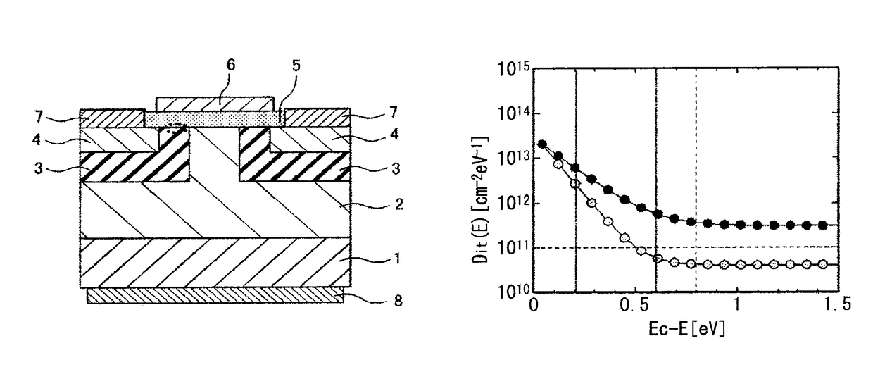
[0034]First, an element structure of a silicon carbide semiconductor device in a first embodiment of the present invention is described. FIG. 1 is a cross-sectional view showing the silicon carbide semiconductor device in the first embodiment of the present invention. In this embodiment, an n-channel silicon carbide MOSFET is described as an example of the silicon carbide semiconductor device.

[0035]As shown in FIG. 1, a drift layer 2 of a first conductivity type is formed on a surface being a first main surface of a silicon carbide substrate 1 of the first conductivity type, and two well regions 3 of a second conductivity type are provided at an interval in a surface layer portion of the drift layer 2. Source regions 4 of the first conductivity type are formed in part of a surface layer portion of the well region 3, and a gate insulating film 5 is formed on part of surfaces of the well regions 3 and the source regions 4. A gate electrode 6 is formed on a surface of the gate insulati...

second embodiment

[0131]FIG. 21 is an enlarged cross-sectional view around a MOS interface of a silicon carbide semiconductor device in a second embodiment. In this embodiment, a gate insulating film 5 includes nitrogen atoms. This embodiment is the same as the first embodiment except for this. This embodiment can further increase a threshold voltage.

[0132]Nitriding receives attention, the nitriding performing a heat treatment on the gate insulating film 5 in an atmosphere of a nitrogen gas such as a nitrogen monoxide (NO) gas and a dinitrogen monoxide (N2O) gas for the purpose of increasing channel mobility of the MOSFET including silicon carbide. The nitriding makes inert interface traps due to surplus C at the MOS surface and increases the channel mobility.

[0133]In this embodiment, after the gate insulating film 5 in FIG. 10 in the first embodiment is formed, the silicon carbide substrate 1 having the structure in FIG. 10 is transferred into a nitriding furnace prior to reoxidation. The temperatur...


PUM


Abstract

A silicon carbide semiconductor device capable of effectively increasing a threshold voltage and a method for manufacturing the silicon carbide semiconductor device. The silicon carbide semiconductor device includes a gate insulating film formed on part of surfaces of the well regions and the source region; and a gate electrode formed on a surface of the gate insulating film so as to be opposite to an end portion of the source region and the well regions. Furthermore, the gate insulating film has, in an interface region between the well regions and the gate insulating film, defects that each form a first trap having an energy level deeper than a conduction band end of silicon carbide and that include a bond between silicon and hydrogen.

Description

TECHNICAL FIELD[0001]The present invention relates to a silicon carbide semiconductor device.BACKGROUND ART[0002]Silicon carbide (SiC) is promising to be a next-generation semiconductor material that can achieve high-voltage, low-loss semiconductor devices. Particularly promising semiconductor devices including silicon carbide are insulated gate semiconductor devices such as metal-oxide-semiconductor field effect transistors (MOSFETs) and insulated gate bipolar transistors (IGBTs) that enable switching operations. The insulated gate semiconductor devices need to have characteristics, namely, normally-off characteristics in which no current passes when voltage is not applied to a gate.[0003]To be used as the semiconductor devices having the normally-off characteristics, semiconductor devices need to have a high threshold voltage (Vth) to some extent, the threshold voltage being a gate voltage when ON-state current starts to flow. For example, IGBTs, which are commonly and commerciall...

Claims


Application Information

Patent Timeline
Patent Type & Authority Patents(United States)
IPC IPC(8): H01L29/40H01L29/10H01L29/06H01L29/78H01L29/739H01L29/66H01L29/16H01L29/51H01L21/04
CPCH01L29/408H01L21/049H01L29/0634H01L29/7802H01L29/518H01L29/1608H01L29/7395H01L29/78H01L29/51H01L29/1095H01L29/66712
Inventor FURUHASHI, MASAYUKIMIURA, NARUHISA
Owner MITSUBISHI ELECTRIC CORP
Why Eureka
Try Eureka