Liquid crystal display device

a liquid crystal display and display screen technology, applied in non-linear optics, instruments, optics, etc., can solve the problems of inefficiency in manufacturing small liquid crystal display devices one by one, damage to polymers in a specific direction with respect to the polarized direction of ultraviolet radiation, and peeling of light shielding films, so as to prevent the reduction of contrast, prevent the effect of reducing the electrical resistance of the light shielding film

Active Publication Date: 2013-04-23
JAPAN DISPLAY INC +1
View PDF12 Cites 7 Cited by
  • Summary
  • Abstract
  • Description
  • Claims
  • Application Information

AI Technical Summary

Benefits of technology

[0019]It is an object of the invention to prevent moisture entering from the outside due to an overcoat film degraded by irradiation of ultraviolet radiation in photo-alignment from affecting a light shielding film.
[0028]According to an aspect of the invention, even when an overcoat film at a seal portion is degraded by ultraviolet radiation in photo-alignment, and moisture penetrates into the degraded overcoat film, the moisture can be blocked by a color filter disposed below the overcoat film and hardly reaches the light shielding film. Therefore, it is possible to prevent the peeling of the light shielding film. Moreover, since a reduction in electrical resistance of the light shielding film can be prevented, it is possible to prevent a reduction in contrast due to light leakage of a liquid crystal layer.
[0029]According to another aspect of the invention, since the overcoat film is formed thicker at the seal portion than at a display region, the overcoat film can be prevented from being entirely degraded by ultraviolet radiation in photo-alignment. Therefore, it is possible to prevent moisture from reaching the light shielding film. Moreover, since the overcoat film is not thick at the display region, it is possible to prevent a reduction in brightness of a display screen.

Problems solved by technology

On the other hand, the liquid crystal display device has a problem of viewing angle characteristics.
For example, when the polymer formed in a network is irradiated with polarized ultraviolet radiation, the polymer in a specific direction with respect to the polarized direction of ultraviolet radiation is damaged.
However, when a portion other than the alignment film is irradiated, the irradiated portion is degraded by the ultraviolet radiation, causing problems.
Manufacturing small liquid crystal display devices one by one is inefficient.
However, such thin glass does not exist as a standard product.
Moreover, such a thin glass substrate cannot undergo the process at present.
This is because irradiation of the alignment films with polarized ultraviolet radiation one by one increases the manufacturing cost.

Method used


Image

  • Liquid crystal display device
  • Liquid crystal display device
  • Liquid crystal display device

Examples


first embodiment

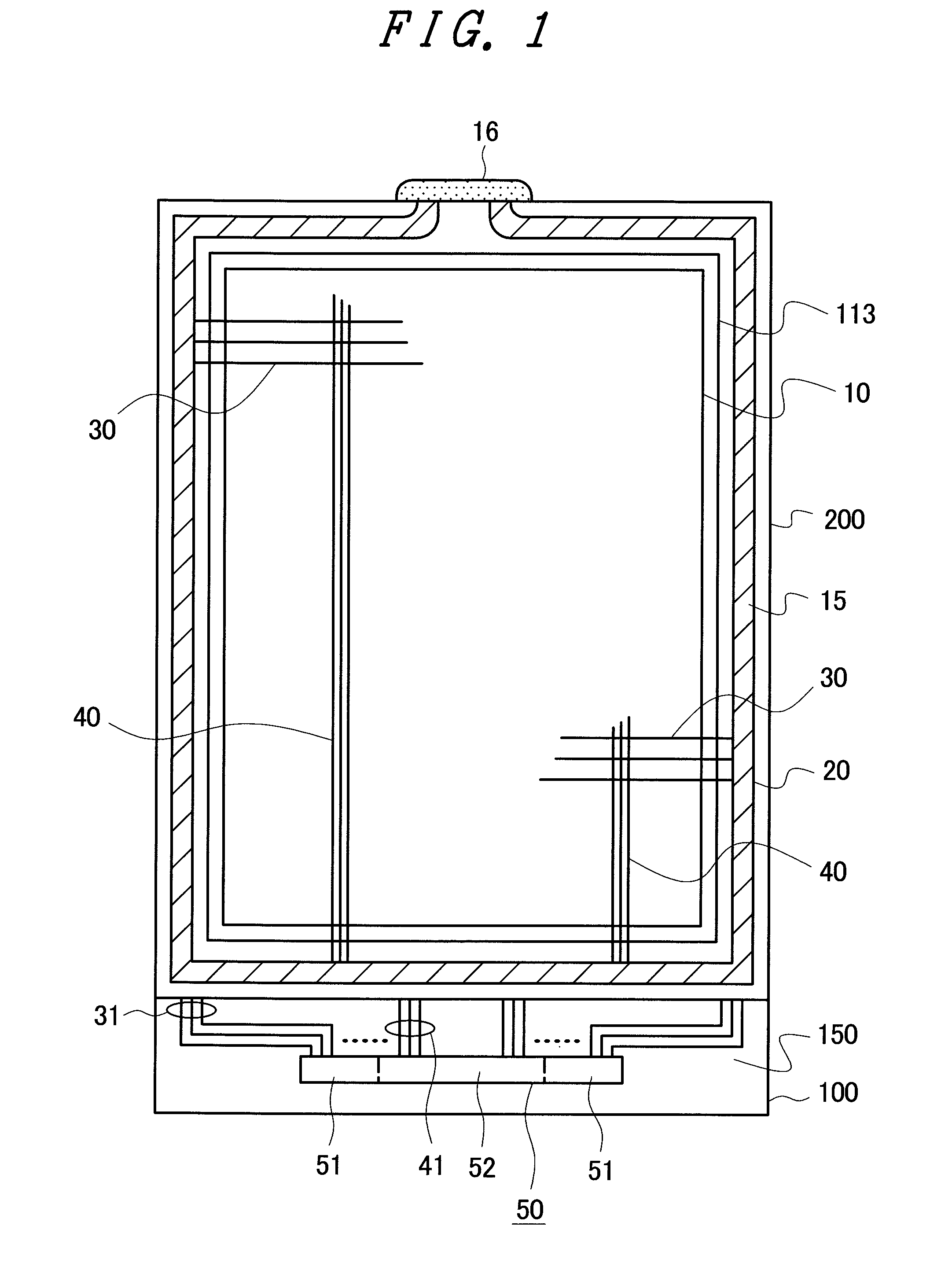
[0048]FIG. 1 is a plan view of a small liquid crystal display device used for mobile phones or the like as an example of a product to which the invention is applied. In FIG. 1, a counter substrate 200 is disposed above a TFT substrate 100. A liquid crystal layer is interposed between the TFT substrate 100 and the counter substrate 200. The TFT substrate 100 and the counter substrate 200 are bonded together with a sealing material 15 formed in a frame portion. In FIG. 1, a filling port is formed in the sealing material 15, and liquid crystal is filled through the filling port. Thereafter, the filling port is sealed with an end-sealing material 16.

[0049]The TFT substrate 100 is formed larger than the counter substrate 200. In a portion of the TFT substrate 100 extended from the counter substrate 200, a terminal portion 150 for supplying a power supply, video signals, scanning signals, and the like to a liquid crystal display panel is formed. In the terminal portion 150, an IC driver 5...

second embodiment

[0073]FIG. 6 is a cross-sectional view of the counter substrate 200 in the vicinity of an edge portion according to a second embodiment of the invention. In FIG. 6, the light shielding film 202, the red color filter 201R, the overcoat film 203, and the alignment film 113 are formed in this order on the counter substrate 200. However, the red color filter 201R and a green color filter 201G are stacked in a seal portion where the alignment film 113 is not present. The alignment film 113 is subjected to the photo-alignment treatment. Accordingly, the overcoat film 203 at the portion where the alignment film 113 is not present is degraded by ultraviolet radiation.

[0074]In FIG. 6, two layers of color filters of the green color filter 201G and the red color filter 201R are formed below the overcoat film 203 degraded by ultraviolet radiation. Accordingly, even when moisture penetrates into the degraded overcoat film 203, the penetrated moisture is blocked by the green color filter 201G and...

third embodiment

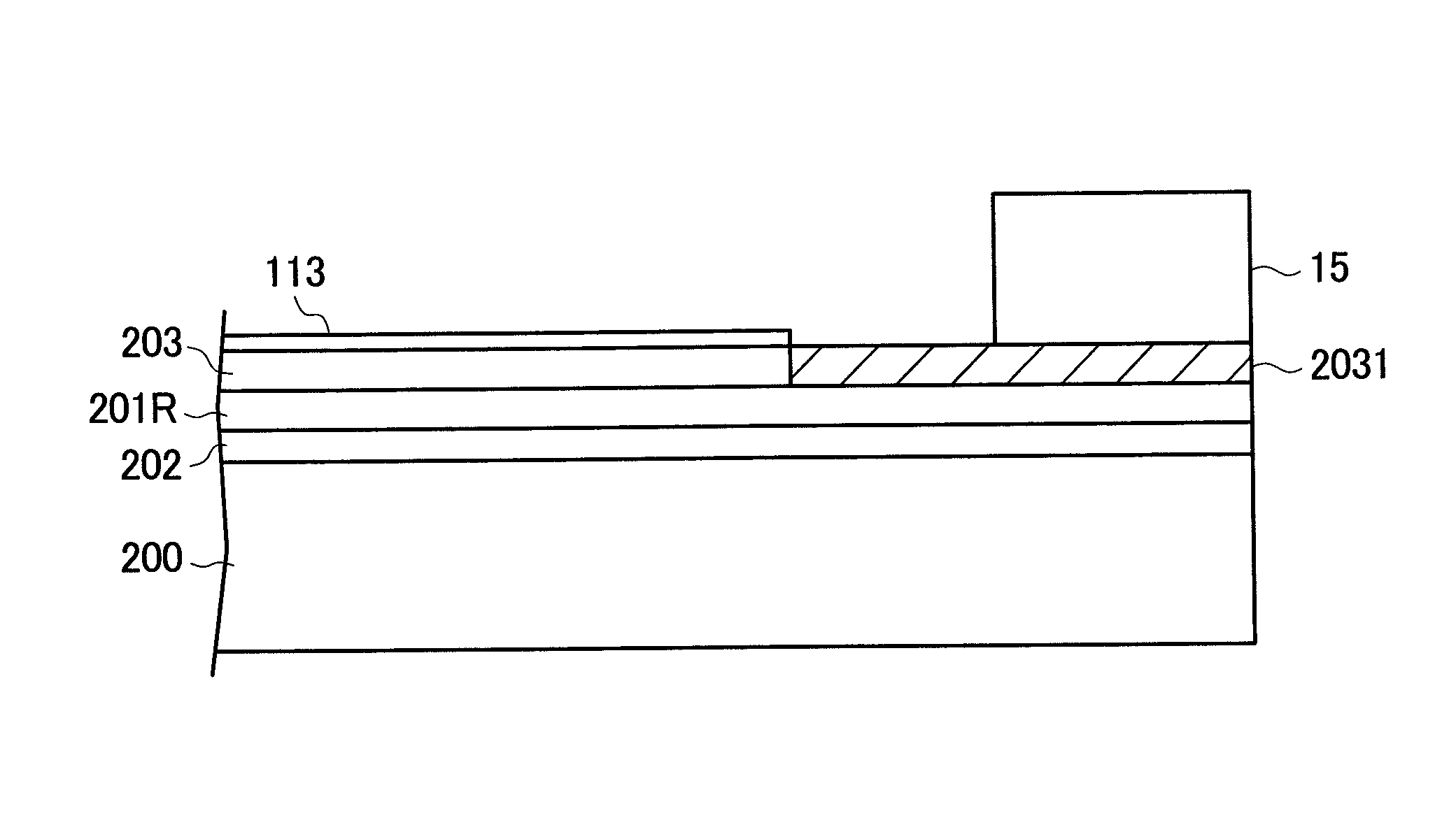
[0082]FIG. 8 is a cross-sectional view of the counter substrate 200 in the vicinity of an edge portion according to a third embodiment. In FIG. 8, the light shielding film 202, the red color filter 201R, the overcoat film 203, and the alignment film 113 are formed in this order on the counter substrate 200. The alignment film 113 is subjected to the photo-alignment treatment. Accordingly, the overcoat film 203 at a portion not covered with the alignment film 113 is degraded by ultraviolet radiation in photo-alignment.

[0083]The red color filter 201R is disposed between the overcoat film 203 degraded by ultraviolet radiation and the light shielding film 202 to thereby block moisture penetrating through the degraded overcoat film 203 by the red color filter 201R in the same manner as in the first embodiment. Different from the first embodiment, the red color filter 201R is not continuously formed to the edge portion in the embodiment. Instead, a region formed by removing the red color ...


PUM

PropertyMeasurementUnit
thicknessaaaaaaaaaa
thicknessaaaaaaaaaa
thicknessaaaaaaaaaa

Abstract

In an IPS type liquid crystal display device, a light shielding film, a red color filter, an overcoat film, and an alignment film are formed in this order on a counter substrate. However, the alignment film is not formed in a seal portion. When the alignment film is subjected to photo-alignment with ultraviolet radiation, a portion of the overcoat film not covered with the alignment film is degraded by ultraviolet radiation. In order to prevent moisture penetrating from the degraded overcoat film from reaching the light shielding film to thereby alter the light shielding film and from causing the peeling of the light shielding film, the red color filter is disposed below the overcoat film to block the moisture.

Description

CLAIM OF PRIORITY[0001]The present application claims priority from Japanese application serial No. 2009-161616 filed on Jul. 8, 2009, the content of which is hereby incorporated by reference into this application.BACKGROUND OF THE INVENTION[0002]1. Field of the Invention[0003]The present invention relates to a display device and more particularly to an in-plane switching (IPS) type liquid crystal display device improved in reliability of a seal portion.[0004]2. Description of the Related Art[0005]A liquid crystal display device includes a TFT substrate on which pixel electrodes, thin film transistors (TFTs), and the like are formed in a matrix, a counter substrate which is disposed to face the TFT substrate and on which color filters and the like are formed at positions corresponding to the pixel electrodes of the TFT substrate, and liquid crystal interposed between the TFT substrate and the counter substrate. An image is formed by controlling the transmittance ratio of light throu...

Claims


Application Information

Patent Timeline
Patent Type & Authority Patents(United States)
IPC IPC(8): G02F1/1339
CPCG02F1/1339G02F1/1368G02F1/1337G02F2001/133519G02F1/134363G02F1/133519G02F1/133512G02F1/133514
Inventor MATSUI, CHIKAESONODA, HIDEHIROKUNIMATSU, NOBORU
Owner JAPAN DISPLAY INC
Why Eureka
Try Eureka