Solid-state imaging device, imaging device and driving method of solid-state imaging device

a solid-state imaging and imaging device technology, applied in the direction of instruments, television systems, television system scanning details, etc., can solve the problems of noise and other problems, and achieve the effects of suppressing dark current, prolonging signal charge accumulation time, and increasing voltage level

Active Publication Date: 2013-06-04
SONY SEMICON SOLUTIONS CORP
View PDF11 Cites 5 Cited by
  • Summary
  • Abstract
  • Description
  • Claims
  • Application Information

AI Technical Summary

Benefits of technology

[0016]A solid-state imaging device to which the above arrangement is applied may be in the form of a single chip or a module having a pixel array section (imaging section) and signal processing section or optical system packaged together. Further, the above arrangement is also applicable to not only a solid-state imaging device but also an imaging device. In this case, the imaging device provides the same advantageous effects as the solid-state imaging device. Here, the imaging device refers, for example, to a camera (or camera system) or a portable device having imaging function. On the other hand, the term “imaging” includes not only image capture during normal camera photography but also, in a board sense, fingerprint detection and others.
[0017]In an embodiment of the present invention, the voltage level of the side to be adjusted is adjusted so that the longer the signal charge accumulation time, the higher the voltage level. This makes it possible to optimally set the voltage level of the side to be adjusted in such a manner as to suppress dark current caused by a leak phenomenon while at the same time meeting the element reliability. It is possible to achieve compatibility between suppressing dark current and ensuring element reliability. What is required is a simple arrangement adapted to adjust the voltage level of the control signal according to the charge accumulation time. Such an arrangement can be implemented without increasing the thickness of the gate oxide film or adversely affecting the transistor manufacturing steps in other ways, thus eliminating the need to increase the number of manufacturing steps.

Problems solved by technology

As a result, noise also becomes a problem.
The side to be adjusted is set to a high voltage level only when the charge accumulation time is long, which is the case where dark current caused by a leak phenomenon becomes a problem.

Method used


Image

  • Solid-state imaging device, imaging device and driving method of solid-state imaging device
  • Solid-state imaging device, imaging device and driving method of solid-state imaging device
  • Solid-state imaging device, imaging device and driving method of solid-state imaging device

Examples


first embodiment

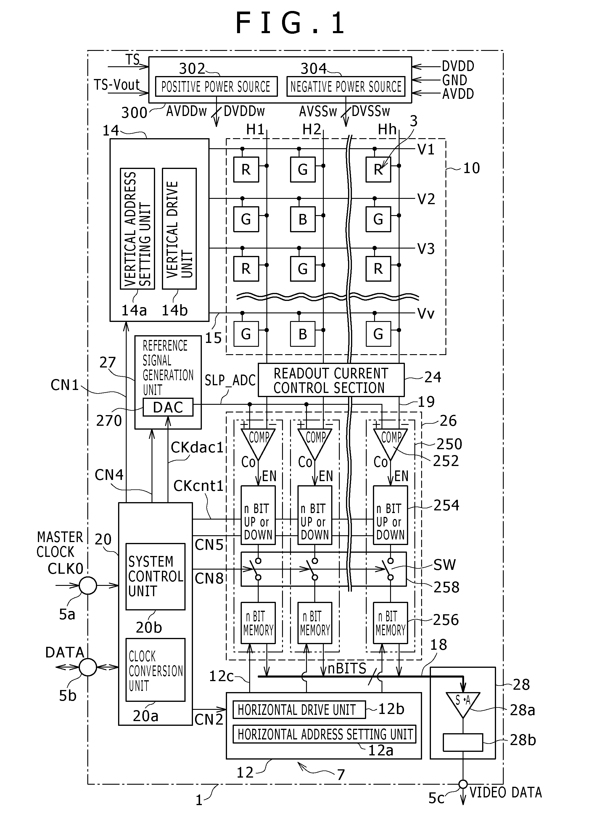
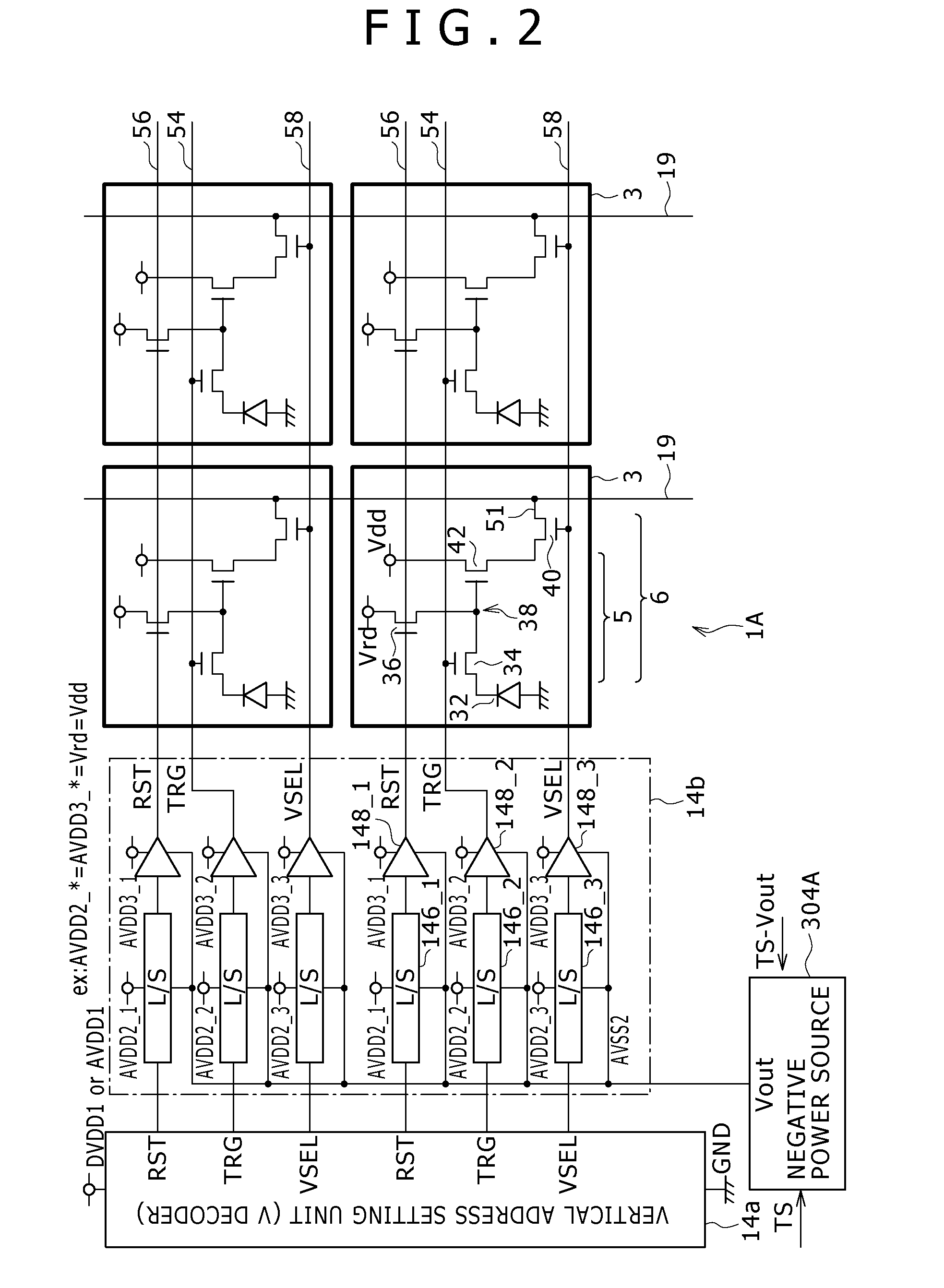
[0061]FIG. 2 is a diagram illustrating a solid-state imaging device 1A according to a first embodiment with focus on the interface between the vertical scan unit 14 and pixel array unit 10. FIG. 2A is a diagram describing a circuit example of an interface portion between the vertical address setting unit 14a and vertical drive unit 14b.

[0062]The unit pixel 3 includes four transistors (readout selection transistor 34, reset transistor 36, vertical selection transistor 40 and amplifying transistor 42), each having a different function, as its basic elements in addition to the charge generation section 32. The readout selection transistor 34, reset transistor 36, and amplifying transistor 42 make up, together with a floating diffusion 38, the pixel signal generation section 5 (signal output section). Then, the pixel signal generation section 5 and vertical selection transistor 40 make up a signal output section 6. The same section 6 generates and outputs the pixel signal voltage Vx fo...

first example

[0095]FIG. 5 is a diagram illustrating a circuit configuration of the negative power source 304 according to a first example adapted to permit negative voltage adjustment shown in FIG. 4. The first example is designed to adjust the feedback voltage Vfb by adjusting the resistance ratio between the resistive elements 342 and 344 while at the same time maintaining the standard voltage Vref0 and reference voltage Vref1 constant, thus adjusting the output voltage Vout.

[0096]More specifically, the second resistive element 344 includes a combination of resistive elements and switches. A resistance R_344 of the second resistive element 344 is adjusted by controlling the on / off operations of the switches, thus adjusting the feedback voltage Vfb and output voltage Vout. The plurality of resistive elements may be arranged in a variety of manners including a series circuit, parallel circuit and series / parallel circuit. The switches are arranged so as to change, as appropriate, the composite re...

second example

[0101]FIG. 5A is a diagram illustrating a circuit configuration of the negative power source 304 according to a second example adapted to permit negative voltage adjustment shown in FIG. 4. The second example is designed to adjust the feedback voltage Vfb and output voltage Vout by adjusting the standard voltage Vref0 while at the same time maintaining the reference voltage Vref1 and the resistance ratio between the resistive elements 342 and 344 constant.

[0102]More specifically, the standard signal generation unit 346 of a negative power source 304_2 according to the second example includes a combination of standard signal generation units 346—x adapted to generate different standard voltages Vref0_x from each other and the switches 348—x (where x=1 to 5 in the figure). The standard signal generation units 346—x and switches 348—x are connected in series. The output voltage control unit 350 includes the control logic 354 adapted to control the switches 348—x. Each of the switches 3...


PUM


Abstract

It is possible to achieve compatibility between suppressing dark current caused by a leak phenomenon and ensuring element reliability in a CMOS solid-state imaging device. When a pixel using electrons as signal charge is driven, the negative voltage level of each of control signals adapted to pulse-drive transistors in the pixel is adjusted so that the longer the charge accumulation time, the higher the voltage level. Preferably, the negative voltage level is grounded (GND) when no signal charge is accumulated. The negative voltage level is increased only when the charge accumulation time is long, which is the case where dark current caused by a leak phenomenon becomes a problem. Therefore, it is possible to suppress stress on the pixels and the gate oxide film of their drive circuits and degradation of the transistor characteristics even if dark current is suppressed.

Description

TECHNICAL FIELD[0001]The present invention relates to a solid-state imaging device, an imaging device and a driving method of the solid-state imaging device. More particularly, the present invention relates to a pixel driving technique suitable for semiconductor devices such as solid-state imaging devices for detecting physical quantity distribution and other electronic equipment which include an arrangement of a plurality of unit pixels sensitive to externally fed electromagnetic waves such as light and radiation, and from which a physical quantity distribution, converted into an electric signal by unit components, can be read out in the form of an electric signal through arbitrary selection by address control.BACKGROUND ART[0002]Semiconductor devices for detecting physical quantity distribution have found wide application in a variety of fields. Such devices have a plurality of unit components (e.g., pixels), sensitive to externally fed electromagnetic waves such as light and radi...

Claims


Application Information

Patent Timeline
Patent Type & Authority Patents(United States)
IPC IPC(8): H04N3/14H04N5/335H01L27/00H04N5/353H04N5/361H04N5/374H04N5/3745
CPCH04N5/2176H04N5/359H04N5/378H04N5/3698H04N5/3741H04N5/361H04N25/63H04N25/62H04N25/709H04N25/766H04N25/75H04N25/76
Inventor KUDO, SHIGETAKA
Owner SONY SEMICON SOLUTIONS CORP
Why Eureka
Try Eureka