
Radiation tolerant complementary cascode switch using non-radiation hardened transistors

a complementary cascade switch and non-radiation hardening technology, applied in the direction of pulse generator, emergency protective arrangement for limiting excess voltage/current, pulse technique, etc., can solve the problems of increased cost, increased production lead time, and correspondingly lower supply

Active Publication Date: 2013-06-04
SUMMER STEVEN E
View PDF22 Cites 6 Cited by
  • Summary
  • Abstract
  • Description
  • Claims
  • Application Information

AI Technical Summary

Benefits of technology

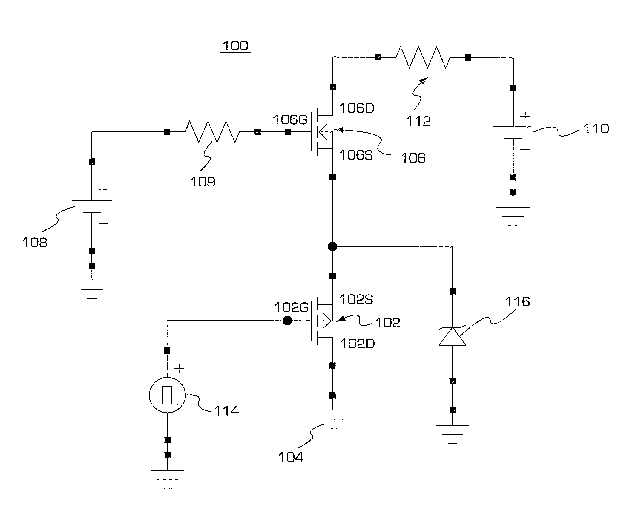
The present invention is a power switching circuit that can be used in radiation environments. It includes two semiconductor switching devices, one of which is a positive threshold voltage and the other is a negative threshold voltage. The second semiconductor switching device is a P-channel FET or an insulated-gate bipolar transistor (IGBT). The circuit has a signal generating circuit that controls the second semiconductor switching device. It can be used to switch power in radiation environments without causing damage to the components.

Problems solved by technology

However, because these components are in limited demand, the supply is correspondingly lower than for similar commercial-grade components.
The limited supply for radiation hardened components leads to increased cost and may increase production lead times. These factors result in higher prices and longer delivery times for the radiation tolerant circuits that incorporate these types of components.
If a conventional non-radiation hardened N-channel FET is used in switching applications where radiation is present, the device tends to fail at relatively low radiation levels because the gate threshold voltage of the N-channel FET shifts more negatively with accumulated radiation dose, and ultimately falls through zero to a negative voltage.
Therefore, the component is difficult to control after the initial application of power.

Method used


Image

  • Radiation tolerant complementary cascode switch using non-radiation hardened transistors
  • Radiation tolerant complementary cascode switch using non-radiation hardened transistors
  • Radiation tolerant complementary cascode switch using non-radiation hardened transistors

Examples


Embodiment Construction

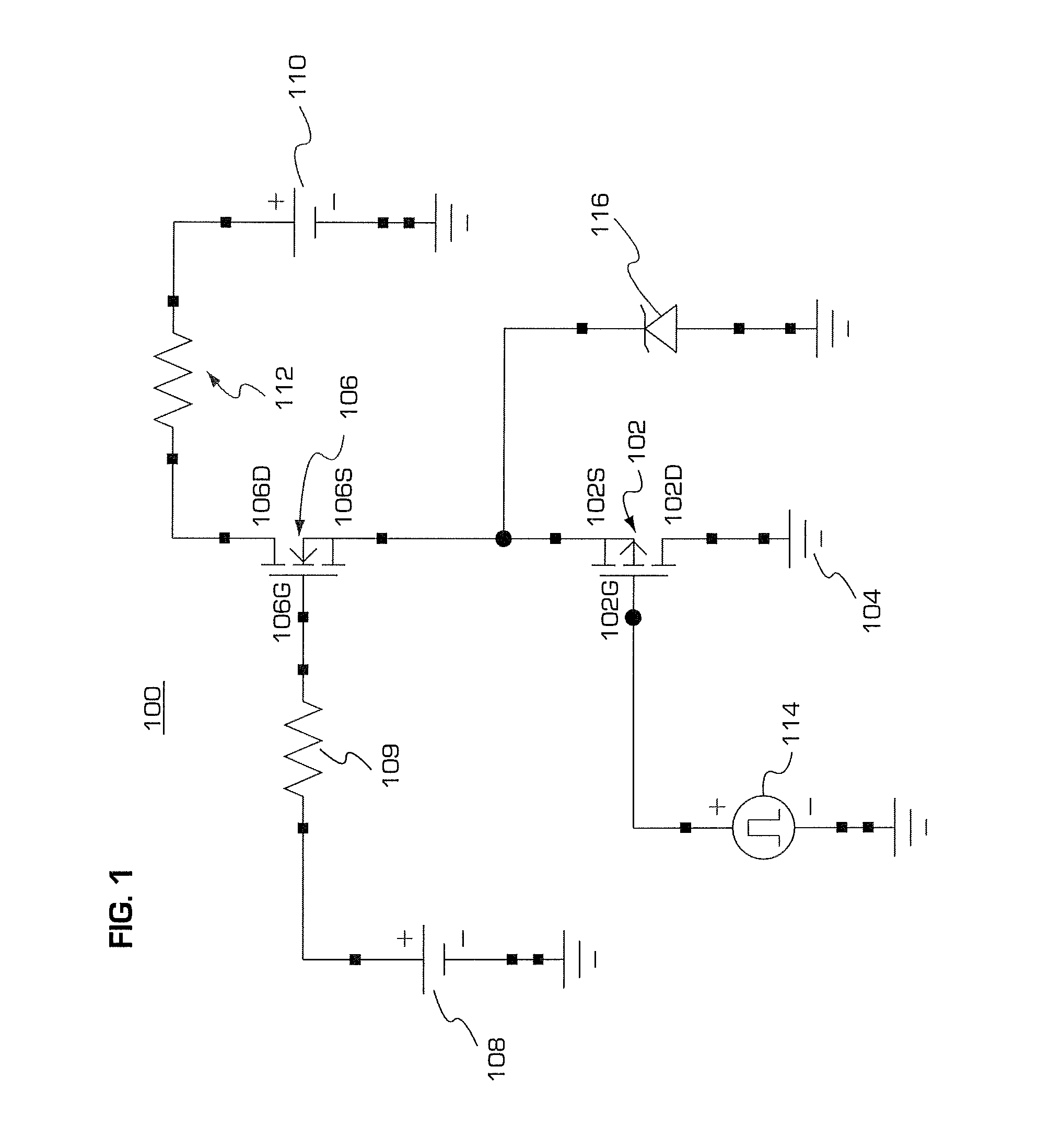
[0017]The present invention provides the ability to use a high voltage rated, non-radiation hardened N-channel FET (N-FET) controlled by a relatively small low voltage, non-radiation hardened P-channel FET (P-FET) while both devices operate within a radiation environment. High voltage in the present invention refers to voltages at or above 50V DC.

[0018]In the present invention, the P-FET device is driven by a sufficiently high drive voltage in order to overcome gate threshold shifts resulting from accumulated radiation damage. This ability of the circuit to operate within design parameters while being exposed to predefined levels of radiation is referred to herein as “radiation tolerance”, and the circuit meeting this criteria, as “radiation tolerant”.

[0019]The ON state, negative gate-to-source drive waveform provided to the P-FET must have a sufficiently large magnitude to saturate the drain-to-source channel. It must, however, not be so high that the gate-to-source breakdown volta...


PUM


Abstract

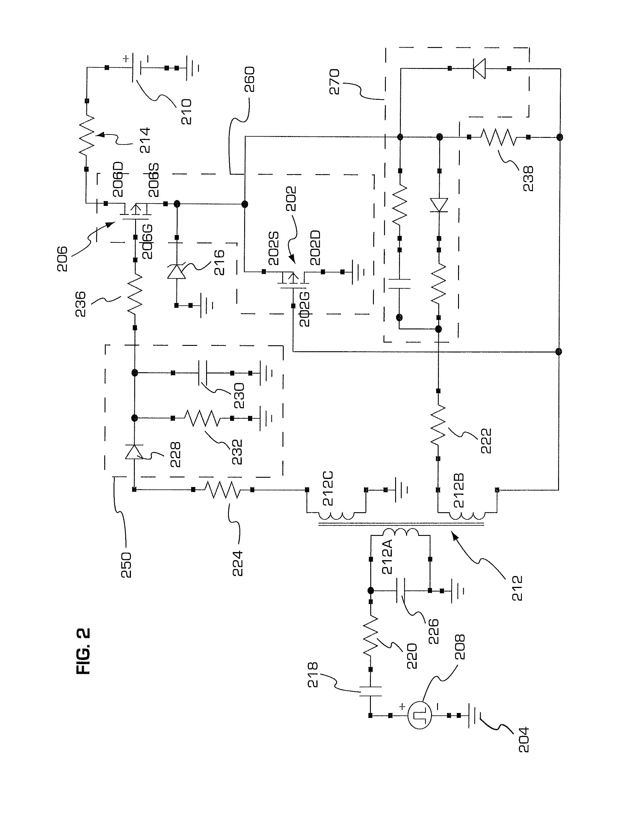
A power switching circuit designed for operating in a radiation environment using non-radiation hardened components is provided. The power switching circuit provides a high-voltage rated, non-radiation hardened N-channel FET (N-FET) controlled by a relatively small, low-voltage, non-radiation hardened P-channel FET (P-FET), while both devices are operating in a radiation environment. The P-FET device is drive by a sufficiently high drive voltage in order to overcome gate threshold shifts resulting from accumulated radiation damage.

Description

FIELD OF THE INVENTION[0001]This invention relates to power switching circuits. More specifically, the invention relates to a radiation tolerant complementary cascade switch using non-radiation hardened transistors.BACKGROUND OF THE INVENTION[0002]One type of field effect transistor (FET) used for power switching is an enhancement mode type FET. An enhancement mode FET is normally non-conducting. However, when a gate voltage above a threshold value is applied, the enhancement mode FET becomes conducting. Additionally, enhancement mode FETs are available in two gate polarities: N-channel and P-channel.[0003]Power switching circuits designed for general purpose use are usually constructed with N-channel FETs because, for any given die size, the N-channel FET has a lower ON resistance than a correspondingly sized P-channel FET would have.[0004]For clarity, several terms used herein are defined. The term “radiation hardened” in the context of the present invention is understood to refer...

Claims


Application Information

Patent Timeline
Patent Type & Authority Patents(United States)
IPC IPC(8): H03K3/00
CPCH03K17/6871H03K17/691H03K2017/0803
Inventor SUMMER, STEVEN E.
Owner SUMMER STEVEN E
Learn More