Thin film encapsulation for flat panel display device and method of manufacturing thin film encapsulation structure

a flat panel display device and thin film technology, applied in the direction of discharge tube luminescnet screens, organic semiconductor devices, transportation and packaging, etc., can solve the problems of encapsulation film not being flexible, high fragility, and affecting the quality of the display unit, so as to reduce the risk of cracks and simplify the manufacturing process

Active Publication Date: 2013-06-11
SAMSUNG DISPLAY CO LTD
View PDF11 Cites 21 Cited by
  • Summary
  • Abstract
  • Description
  • Claims
  • Application Information

AI Technical Summary

Benefits of technology

[0011]Aspects of embodiments of the present invention provide thin film encapsulation for a flat panel display device and a method of manufacturing a thin film encapsulation structure, which simplifies the manufacturing process and reduces a risk of cracks occurring.

Problems solved by technology

Display units of the organic light emitting display device type may deteriorate due to penetration of oxygen or water.
While the order of forming organic and inorganic layers may be modified, since the substrate is moved from or to the chambers for depositing an organic layer and an inorganic layer, the manufacturing process may be considerably burdensome and complicated.
However, in this case, this thin film encapsulation film may not be flexible and have high fragility, and even when a small particle is mixed thereinto, stress around the particle may be concentrated and create cracks.

Method used


Image

  • Thin film encapsulation for flat panel display device and method of manufacturing thin film encapsulation structure
  • Thin film encapsulation for flat panel display device and method of manufacturing thin film encapsulation structure
  • Thin film encapsulation for flat panel display device and method of manufacturing thin film encapsulation structure

Examples


Embodiment Construction

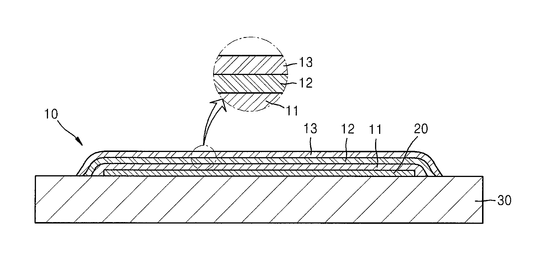
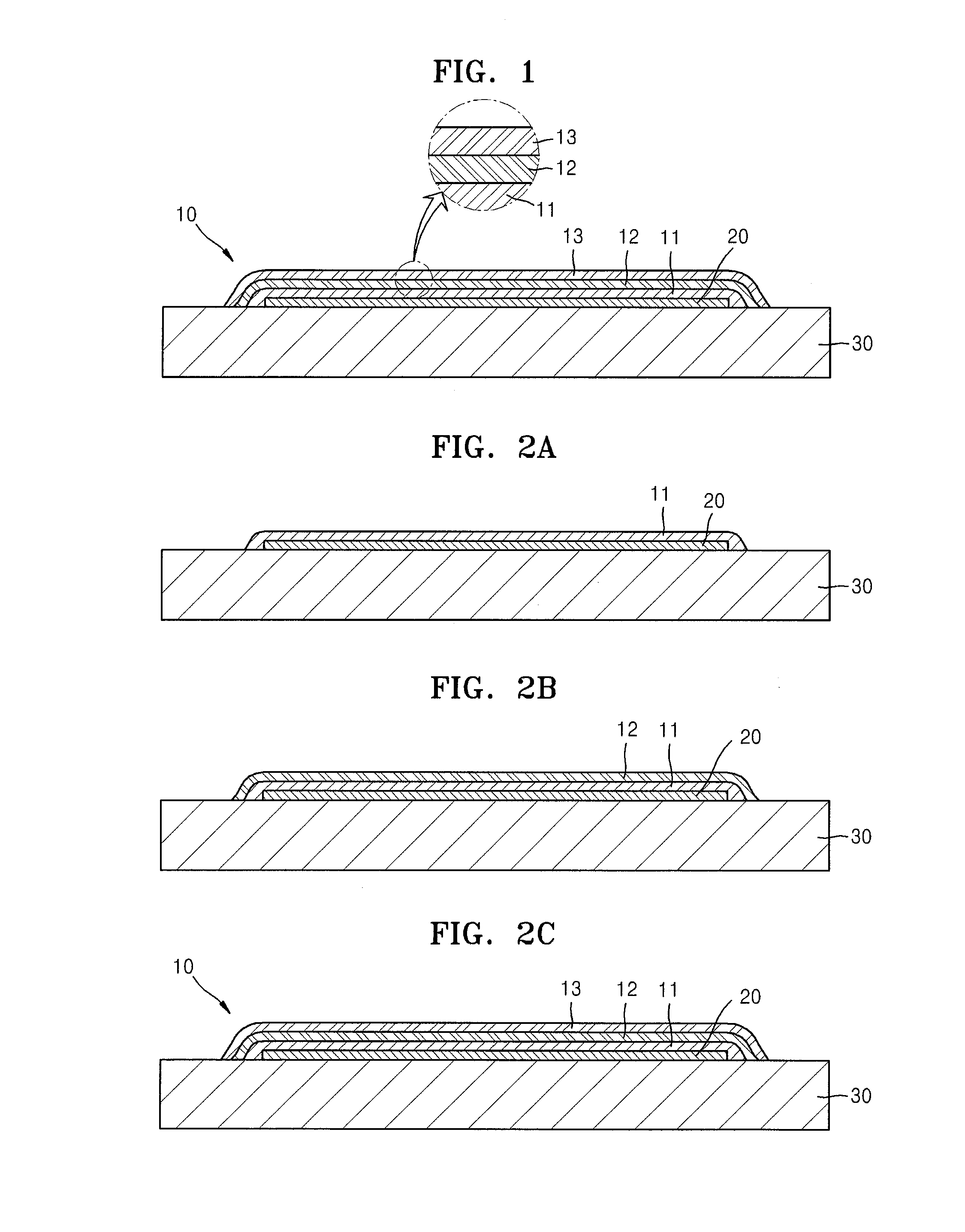
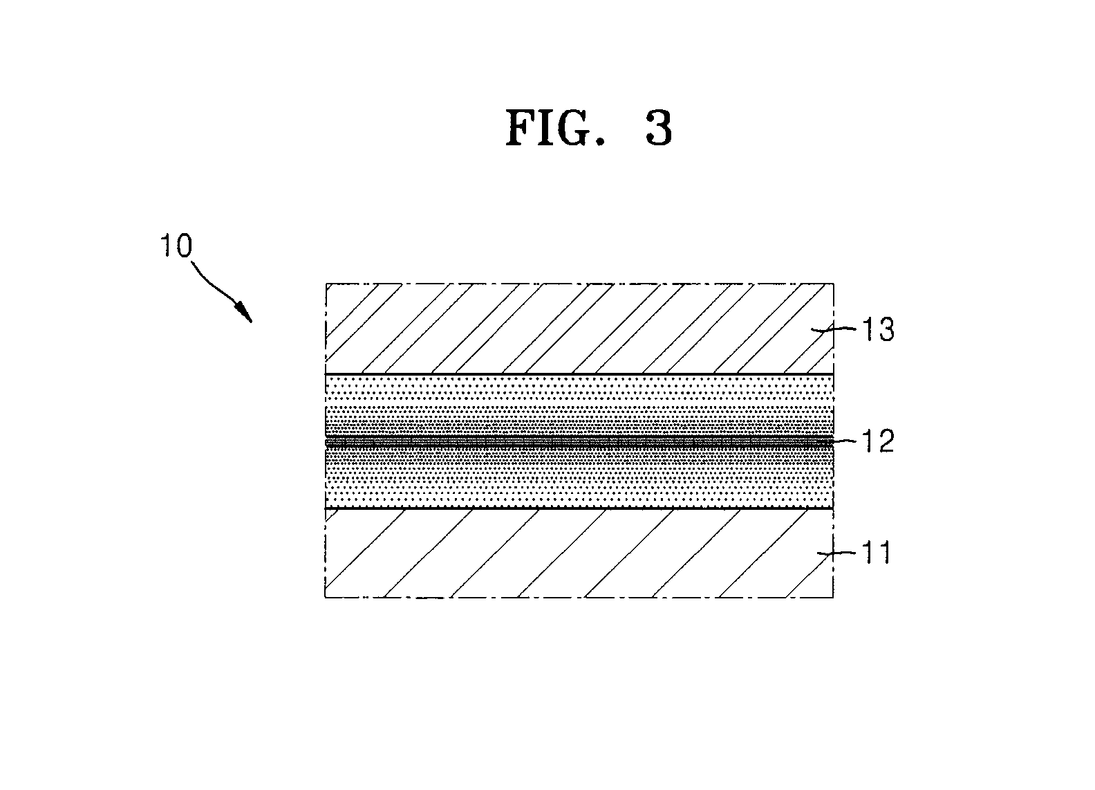
[0029]Aspects of embodiments of the present invention will now be described more fully with reference to the accompanying drawings, in which exemplary embodiments of the invention are shown. The present invention may, however, be embodied in many different forms and should not be construed as being limited to the embodiments set forth herein; rather, these embodiments are provided so that this disclosure will be thorough and complete, and will fully convey the concept of the invention to those skilled in the art. The terminology used herein is for the purpose of describing particular embodiments only, and is not intended to be limiting. In addition, when an element is referred to as being “on” another element, it may be directly on the another element or may be indirectly on the another element with one or more intervening elements interposed therebetween.

[0030]A thin film encapsulation for a flat panel display device and method of manufacturing the same according to exemplary embod...


PUM


Abstract

Thin film encapsulation for a flat panel display device and a method of manufacturing the thin film encapsulation structure. The thin film encapsulation structure of the flat panel display device includes thin film layers covering a display unit formed on a substrate, wherein the thin film layers comprise a plurality of inorganic layers and a hexamethyldisiloxane (HMDSO) layer interposed between the inorganic layers. Accordingly, as multiple layers of the thin film encapsulation structure may be formed in a single chamber, the manufacturing process may be simplified, and also, as the HMDSO layer, which is flexible, absorbs stresses, a risk of cracks occurring may also be reduced.

Description

CROSS-REFERENCE TO RELATED PATENT APPLICATION[0001]This application claims priority to and the benefit of Korean Patent Application No. 10-2012-0052595, filed on May 17, 2012, in the Korean Intellectual Property Office, the disclosure of which is incorporated herein in its entirety by reference.BACKGROUND[0002]1. Field[0003]Aspects of the present invention relate generally to a thin film encapsulation structure for a flat panel display device and a method of manufacturing the thin film encapsulation structure.[0004]2. Description of the Related Art[0005]A flat panel display device, such as an organic light emitting display device, may be thin and flexible due to characteristics thereof, and, thus, research is being conducted into flat panel display devices, such as the organic light emitting display device.[0006]Display units of the organic light emitting display device type may deteriorate due to penetration of oxygen or water. Thus, in order to prevent or reduce the penetration of...

Claims


Application Information

Patent Timeline
Patent Type & Authority Patents(United States)
IPC IPC(8): H05B33/04
CPCH01L51/5256Y10T428/23H01L2251/5338H10K50/8445H10K2102/311H05B33/04H10K71/00
Inventor OH, MIN-HOCHO, YOON-HYEUNGKIM, YONG-TAKLEE, SO-YOUNGCHO, SANG-HWANLEE, BYOUNG-DUKJUNG, SUN-YOUNGCHUNG, YUN-AHKIM, SOO-YOUNKIM, DONG-JINMOON, JI-YOUNGSONG, SEUNG-YONGLEE, JONG-HYUK
Owner SAMSUNG DISPLAY CO LTD
Why Eureka
Try Eureka