CMOS image sensor having global shutter pixels built using a buried channel transfer gate with a surface channel dark current drain

a technology of dark current drain and buried channel transfer gate, which is applied in the direction of electrical equipment, semiconductor devices, radio frequency control devices, etc., can solve the problems of significant degrading of sensor performance, and achieve the effects of low dark current, low power supply voltage, and small pixel siz

Active Publication Date: 2013-06-25
APTINA IMAGING CORP
View PDF4 Cites 33 Cited by
  • Summary
  • Abstract
  • Description
  • Claims
  • Application Information

AI Technical Summary

Benefits of technology

[0009]It is an object of the disclosed invention to overcome limitations in the prior art. It is a further object of the disclosed invention to provide a practical CMOS image sensor design that has a small pixel size, can operate in the rolling shutter mode as well as in the global shutter mode with low dark current, and with low power supply voltage. One possibility described in this disclosure is to use a transfer gate for charge storage. However, the standard transfer gate has a problem of large dark current generation at the interface between the silicon and silicon-dioxide, which would significantly degrade the sensor performance. It is therefore desirable to provide a novel transfer gate which incorporates two charge channels in a stacked fashion above each other where the shallow channel collects the dark current and drains it away thus preventing signal degradation, while the underlying bulk charge transfer channel is used for charge transfer and storage of charge from the PD and also transfers it into the FD during the readout sequence in the standard way.

Problems solved by technology

However, the standard transfer gate has a problem of large dark current generation at the interface between the silicon and silicon-dioxide, which would significantly degrade the sensor performance.

Method used


Image

  • CMOS image sensor having global shutter pixels built using a buried channel transfer gate with a surface channel dark current drain
  • CMOS image sensor having global shutter pixels built using a buried channel transfer gate with a surface channel dark current drain
  • CMOS image sensor having global shutter pixels built using a buried channel transfer gate with a surface channel dark current drain

Examples


Embodiment Construction

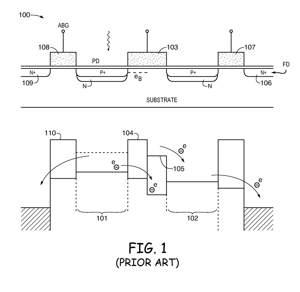
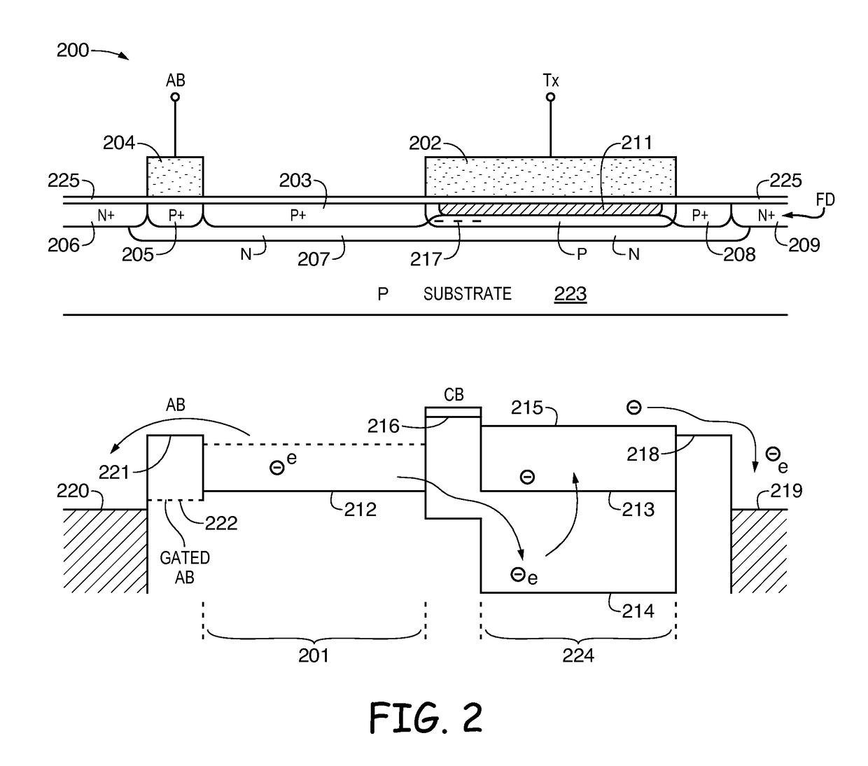
[0018]The drawing 200 in FIG. 2 is a simplified cross section of a pixel of the present invention with associated simplified potential diagram drawn in the direction from the PD to the FD. The pixel consists of a pinned photodiode region 201, the transfer-storage gate region (TX) 202, the storage well (SW) region 224, the pinned barrier region (PB) 208, and the FD region 209. The p substrate 223 has a p+ doped layer 203 placed close to its surface that forms a part of the pinned photodiode PD. Another n doped layer 207 is shown extending from the PD under the transfer-storage gate region TX and under the p+ pinned charge transfer barrier (PB) 208 all the way to the FD region 209. The entire surface of the pixel is covered by an oxide layer 225 that isolates the TX gate 202 from the substrate 223. Another gate 204 can be placed adjacent to the pinned photodiode 201 that serves as a PD reset gate. This gate 204 also establishes the potential barrier 221 for the blooming control. When ...


PUM


Abstract

The invention describes a solid-state CMOS image sensor array and in particular describes in detail image sensor array pixels having global and rolling shutter capabilities that are using a dual channel transfer-storage gate for charge transfer from a PD to a TX gate well and from the TX gate well onto a FD. The dual channels are stacked above each other where a shallow charge channel is used to drain surface generated dark current away from the pixel structure, while a buried bulk channel provides for standard charge transfer and storage functions. This feature thus improves the sensor noise performance and prevents signal contamination and various shading effects caused by the dark current buildup during a prolonged charge storage sequence in pixels of image sensor arrays using the global shutter mode of operation. Several embodiment of this concept are described including pixels which utilize shared circuitry, a complete PD reset capability, and an efficient anti-blooming control.

Description

CROSS REFERENCE TO RELATED APPLICATION[0001]This applications claims priority under 35 USC Sec. 119 (e)(1) of provisional application No. 61 / 438,111 filed on Jan. 31, 2011.BACKGROUND OF THE INVENTION[0002]1. Field of the Invention[0003]The disclosed invention relates to solid-state image sensors and more specifically to small pixel size CMOS image sensors that have global shutter (GS) and rolling shutter (RS) capabilities.[0004]2. Description of Related Art[0005]Typical image sensors sense light by converting impinging photons into electrons that are integrated (collected) in the sensor pixels. After completion of the integration cycle collected charge is converted into a voltage, which is supplied to the output terminals of the sensor. In CMOS image sensors the charge to voltage conversion is accomplished directly in the pixels themselves and the analog pixel voltage is transferred to the output terminals through various pixel addressing and scanning schemes. The analog signal can ...

Claims


Application Information

Patent Timeline
Patent Type & Authority Patents(United States)
IPC IPC(8): H01L31/062H01L31/113
CPCH01L27/14603H01L27/14612H01L27/14641H01L31/103
Inventor HYNECEK, JAROSLAVKOMORI, HIROFUMI
Owner APTINA IMAGING CORP
Why Eureka
Try Eureka