
Array-based integrated circuit with reduced proximity effects

a technology of proximity effects and arrays, applied in cad circuit design, total factory control, instruments, etc., can solve the problems of increasing the manufacturing cost of the integrated circuit containing the memory, increasing the manufacturing cost of the integrated circuit, and increasing the proximity effect of the transistors. the effect of proximity effects between array edge devices and interior devices

Active Publication Date: 2013-06-25
TEXAS INSTR INC
View PDF3 Cites 1 Cited by
  • Summary
  • Abstract
  • Description
  • Claims
  • Application Information

AI Technical Summary

Benefits of technology

This approach effectively reduces proximity effects between edge and interior devices, enhancing the performance consistency of memory and logic arrays while eliminating the need for costly dummy cells, thus improving yield and reducing manufacturing costs.

Problems solved by technology

But at those small feature sizes, transistors become more sensitive to proximity effects.
In many memory designs, yield analysis has shown preponderance for data storage failures (failed read or failed write) for memory cells at array edges, as compared with interior cells.
Of course, the chip area required for these memory cells adds to the manufacturing cost of the integrated circuit containing the memory.
Other types of integrated circuit functions that are also constructed as an array or region of repetitive device structures, similarly suffer from device variations due to proximity effect.

Method used


Image

  • Array-based integrated circuit with reduced proximity effects
  • Array-based integrated circuit with reduced proximity effects
  • Array-based integrated circuit with reduced proximity effects

Examples


Embodiment Construction

[0032]This invention will be described in connection with one or more of its embodiments, namely as implemented into an integrated circuit including a solid-state memory array, as it is contemplated that this invention will be especially beneficial when realized in that application. However, it is also contemplated that this invention can provide important benefit in other applications, for example in integrated circuits including a logic array, such as a regular array of transistors, gates, or logic cells. Accordingly, it is to be understood that the following description is provided by way of example only, and is not intended to limit the true scope of this invention as claimed.

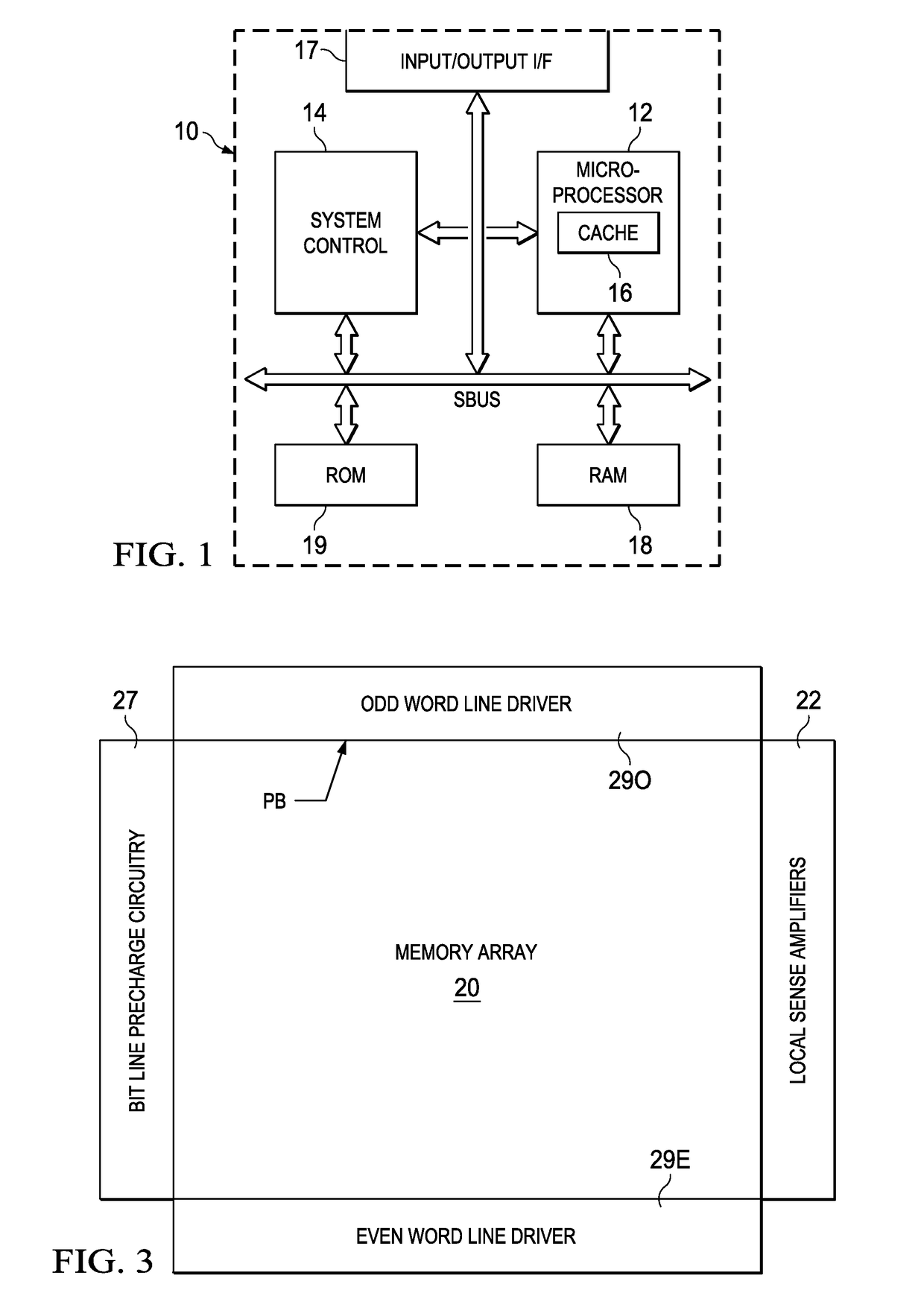
[0033]FIG. 1 illustrates an example of large-scale integrated circuit 10, in the form of a so-called “system-on-a-chip” (“SoC”), as now popular in many electronic systems. Integrated circuit 10 is a single-chip integrated circuit into which an entire computer architecture is realized. As such, in this examp...


PUM


Abstract

An integrated circuit and method of generating a layout for an integrated circuit in which circuitry peripheral to an array of repetitive features, such as memory or logic cells, is realized according to devices constructed similarly as the cells themselves, in one or more structural levels. The distance over which proximity effects are caused in various levels is determined. Those proximity effect distances determine the number of those features to be repeated outside of and adjacent to the array for each level, within which the peripheral circuitry is constructed to match the construction of the repetitive features in the array.

Description

CROSS-REFERENCE TO RELATED APPLICATIONS[0001]This application is a division of application Ser. No. 12 / 913,479, filed Oct. 27, 2010, the contents of which are hereby incorporated by reference.STATEMENT REGARDING FEDERALLY SPONSORED RESEARCH OR DEVELOPMENT[0002]Not applicable.BACKGROUND OF THE INVENTION[0003]This invention is in the field of solid-state integrated circuits, and is more specifically directed to the layout and arrangement of device arrays and peripheral circuitry in such integrated circuits.[0004]Many modern electronic devices and systems now include substantial computational capability for controlling and managing a wide range of functions and useful applications. The computational power of these modern devices and systems is typically provided by one or more processor “cores”. These processor cores operate as a digital computer, in general retrieving executable instructions from memory, performing arithmetic and logical operations on digital data retrieved from memor...

Claims


Application Information

Patent Timeline
Patent Type & Authority Patents(United States)
IPC IPC(8): G11C5/02G06F17/50
CPCG06F17/5068G06F17/5081G11C5/025G06F2217/12G06F30/39G06F30/398G06F2119/18Y02P90/02
Inventor DENG, XIAOWEILOH, WAH KITSESHADRI, ANANDBLAKE, TERENCE G. W.
Owner TEXAS INSTR INC
Learn More