Assembly of multi-chip modules using sacrificial features

a technology of multi-chip modules and features, applied in electrical apparatus, semiconductor devices, semiconductor/solid-state device details, etc., can solve the problems of poor manufacturing throughput, difficulty in increasing difficulties, and difficulty in achieving 1-3 m accuracy of flip-chip bonders, and achieve the effect of facilitating electrical coupling of components

Active Publication Date: 2013-07-16
ORACLE INT CORP
View PDF1 Cites 2 Cited by
  • Summary
  • Abstract
  • Description
  • Claims
  • Application Information

AI Technical Summary

Benefits of technology

[0011]Furthermore, the first surface may include a first negative feature and the second surface may include a second negative feature. The positive feature may mate with the first negative feature and the second negative feature, thereby facilitating the alignment. For example, the first negative feature and the second negative feature may include pits, and the positive feature may include the spherically shaped coupling component.
[0014]Note that the alignment may facilitate electrical coupling of components on the first substrate and the second substrate using a through-silicon via (TSV). Moreover, the bulk modulus of the first material may be less than a bulk modulus of a metal connector in the TSV.

Problems solved by technology

In existing 3D chip stacking TSV techniques, chip-to-wafer and / or chip-to-chip bonding remains a challenging operation because of problems in attaining ultra-high alignment accuracy and high-throughput manufacturing.
These difficulties are expected to increase in future multi-chip systems.
However, existing flip-chip bonders, which can achieve an accuracy of ±1-3 μm, usually have poor manufacturing throughput.
Similarly, other alignment techniques that ensure high bonding accuracy are typically not suitable for use in high-volume manufacturing because of the long time needed to bond a single chip.
Indeed, low manufacturing throughput often makes bonding one of the most expensive process operations when fabricating TSVs, which, in turn, increases the cost of the resulting multi-chip systems.

Method used


Image

  • Assembly of multi-chip modules using sacrificial features
  • Assembly of multi-chip modules using sacrificial features
  • Assembly of multi-chip modules using sacrificial features

Examples


Embodiment Construction

[0026]The following description is presented to enable any person skilled in the art to make and use the disclosure, and is provided in the context of a particular application and its requirements. Various modifications to the disclosed embodiments will be readily apparent to those skilled in the art, and the general principles defined herein may be applied to other embodiments and applications without departing from the spirit and scope of the present disclosure. Thus, the present disclosure is not intended to be limited to the embodiments shown, but is to be accorded the widest scope consistent with the principles and features disclosed herein.

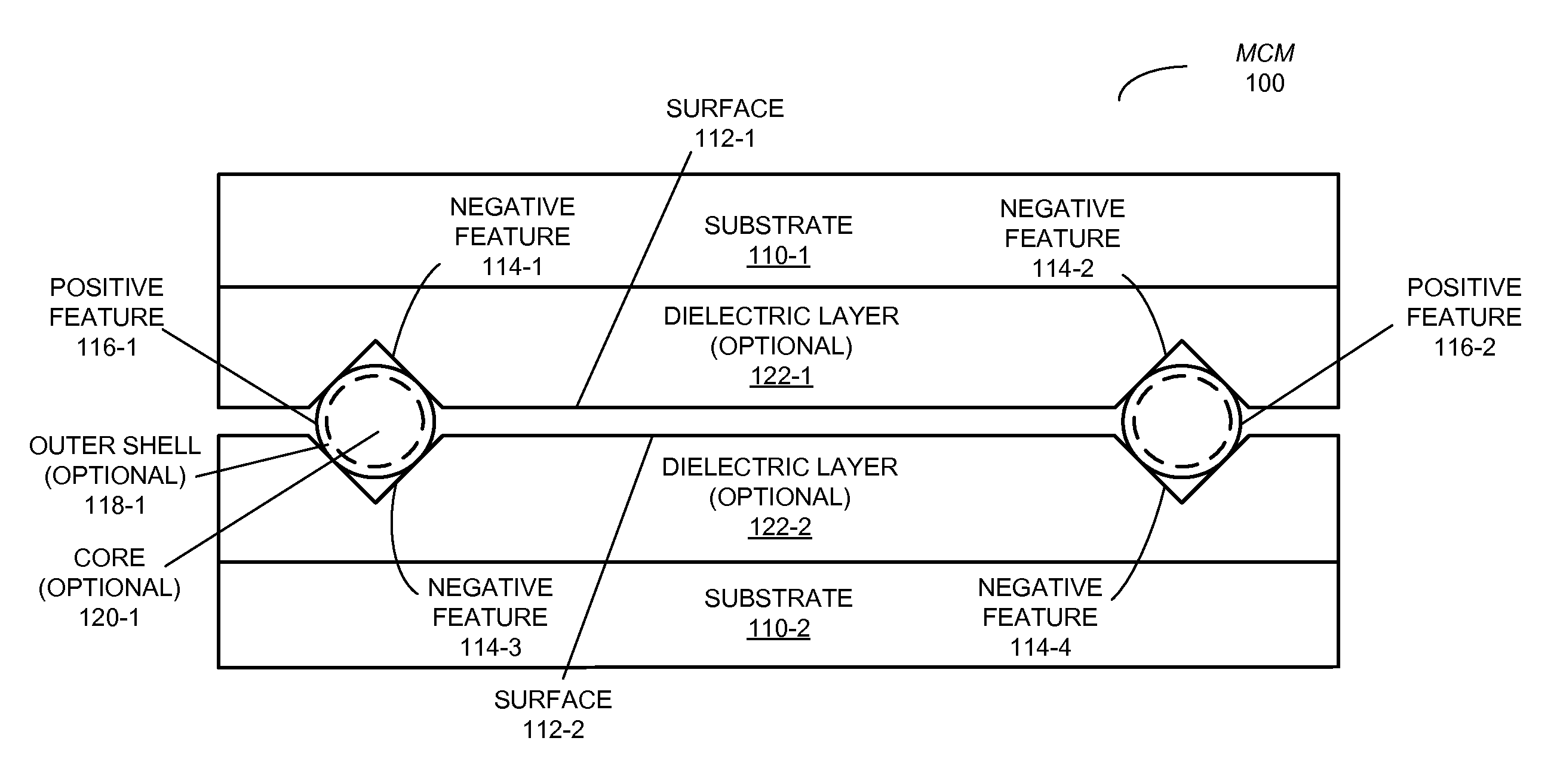
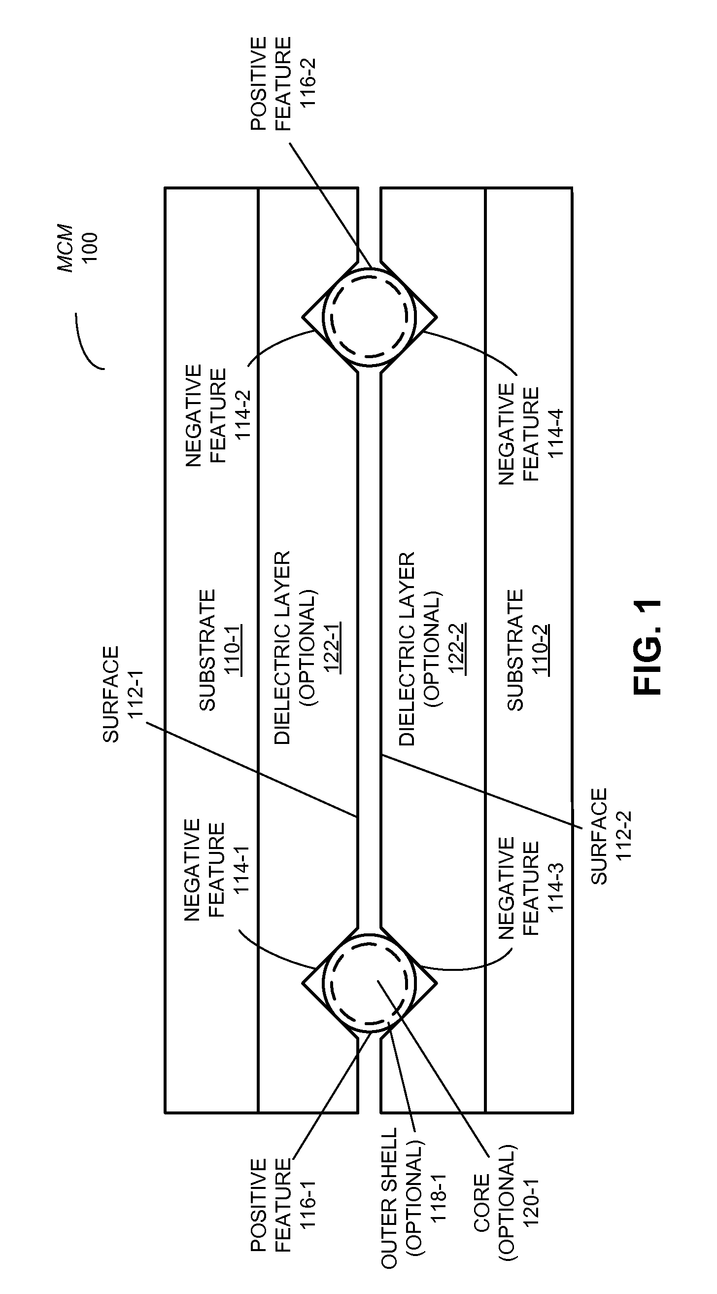
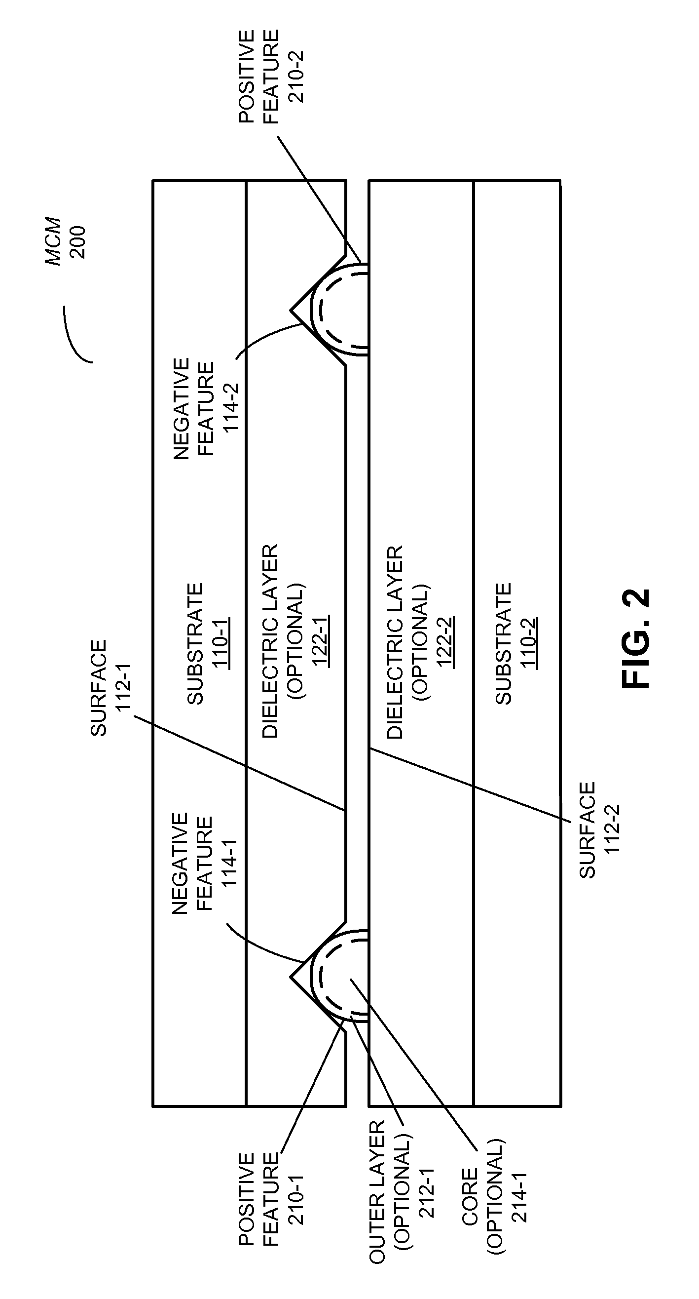
[0027]Embodiments of a multi-chip module (MCM), an electronic device that includes the MCM, and a technique for assembling the MCM are described. This MCM includes two substrates, having facing surfaces, which are mechanically coupled. Disposed on a surface of a first of these substrates, there is a negative feature, which is recessed below ...


PUM


Abstract

A multi-chip module (MCM) is described. This MCM includes two substrates, having facing surfaces, which are mechanically coupled. Disposed on a surface of a first of these substrates, there is a negative feature, which is recessed below this surface. A positive feature in the MCM, which includes an assembly material other than a bulk material in the substrates, at least in part mates with the negative feature. For example, the positive feature may be disposed on the surface of the other substrate. Alternatively, prior to assembly of the MCM, the positive feature may be a separate component from the substrates (such as a micro-sphere). Note that the assembly material has a bulk modulus that is less than a bulk modulus of the material in the substrates. Furthermore, at least a portion of the positive feature may have been sacrificed when the mechanical coupling was established.

Description

BACKGROUND[0001]1. Field[0002]The present disclosure generally relate to a multi-chip modules (MCMs) for semiconductor chips. More specifically, the present disclosure relates to an MCM that includes features that are at least partially sacrificed during assembly of the MCM.[0003]2. Related Art[0004]Three dimensional (3D) chip stacking using through-silicon-vias (TSVs) is an important area of research in developing future high-density, high-performance multi-chip systems. In existing 3D chip stacking TSV techniques, chip-to-wafer and / or chip-to-chip bonding remains a challenging operation because of problems in attaining ultra-high alignment accuracy and high-throughput manufacturing. These difficulties are expected to increase in future multi-chip systems.[0005]For example, in proposed multi-chip systems, die stacking is expected to be implemented in the metal layers below the top metal bond pads, and the target pad size / pitch is expected to decrease from 50-200 μm to 5-10 μm. Furt...

Claims


Application Information

Patent Timeline
Patent Type & Authority Patents(United States)
IPC IPC(8): H01L23/34
CPCH01L23/544H01L24/13H01L24/81H01L25/0657H01L25/50H01L21/6835H01L2924/00011H01L2224/1319H01L2224/13147H01L2224/131H01L2924/014H01L2924/01033H01L2924/01006H01L24/05H01L24/83H01L24/90H01L2223/54426H01L2223/54473H01L2224/13021H01L2224/13099H01L2224/81001H01L2224/81203H01L2224/81801H01L2224/90H01L2225/06513H01L2225/06593H01L2924/01029H01L2924/09701H01L2924/00014H01L2224/83851H01L2224/0401
Inventor SHI, JINGDOUGLAS, DAVID C.
Owner ORACLE INT CORP
Why Eureka
Try Eureka