
Direct IMS (injection molded solder) without a mask for forming solder bumps on substrates

a technology of injection molding and solder, which is applied in the direction of resist details, lithographic masks, non-printed masks, etc., can solve the problems of flux application, reduced solder balls b>2008/b> may be expensive, and limited commercial applications of the solder paste stencil printing method

Active Publication Date: 2013-07-23
GLOBALFOUNDRIES U S INC
View PDF23 Cites 11 Cited by
  • Summary
  • Abstract
  • Description
  • Claims
  • Application Information

AI Technical Summary

Benefits of technology

This approach enables the formation of high volume solder bumps on fine pitch substrates with reduced process steps and costs, achieving solder bumps with heights above the solder resist surface, even in nitrogen environments, which can eliminate the need for additional reflow processes.

Problems solved by technology

However, commercial applications of the solder paste stencil printing method are limited to substrates with pitches greater than or equal to 150 microns because the high volume percentage of flux (around 50 volume %) in the solder paste hinders formation of high volume solder bumps without solder bridging.
Solder balls 2008 may be expensive and flux application and solder ball dispensing may be somewhat complex.

Method used


Image

  • Direct IMS (injection molded solder) without a mask for forming solder bumps on substrates
  • Direct IMS (injection molded solder) without a mask for forming solder bumps on substrates
  • Direct IMS (injection molded solder) without a mask for forming solder bumps on substrates

Examples


Embodiment Construction

[0021]Initially, the complete disclosure of U.S. patent application Ser. No. 12 / 269,240 of Gruber et al., filed Nov. 12, 2008, entitled “Injection Molded Solder Method for Forming Solder Bumps on Substrates” (“the '240 application”) is expressly incorporated herein by reference in its entirety for all purposes. FIGS. 3A-3F depict certain techniques of the '240 application. Attention should now be given to FIGS. 3A and 3B. As seen therein, a mask 102 includes a plurality of through holes 104 arranged in a desired pattern. The mask 104 is located adjacent a substrate 106. The substrate may be, for example, an organic substrate with a plurality of wet-able pads 108 (for example, copper, gold, nickel, and the like) located in recesses. The mask may be, for example, a polyimide film or a thin material that does not react with solder (e.g., non-wetting metals such as molybdenum, stainless steel, aluminum, and the like). As shown in FIG. 3A, the mask 102 is aligned to the substrate 106 so ...


PUM

PropertyMeasurementUnit
distanceaaaaaaaaaa
thicknessaaaaaaaaaa
thicknessaaaaaaaaaa

Abstract

An assembly is obtained; it includes a substrate; a plurality of wet-able pads formed on a surface of the substrate; and a solder resist layer deposited on the surface of the substrate and having an outer surface. At least the solder resist layer is formed with recessed regions defining volumes adjacent the wet-able pads. Molten solder is directly injected into the volumes adjacent the wet-able pads, such that the volumes adjacent the wet-able pads are filled with solder. The solder is allowed to solidify. It forms a plurality of solder structures adhered to the wet-able pads. The substrate and the solder are re-heated after the solidification, to re-flow the solder into generally spherical balls extending above the outer surface of the solder resist layer. The volumes adjacent the wet-able pads are configured and dimensioned to receive sufficient solder in the injecting step such that the generally spherical balls extend above the outer surface of the solder resist layer as a result of the re-heating step. In an alternative approach, solder injection and solidification are carried out in a nitrogen environment or a forming gas environment, and the reflow step may be omitted.

Description

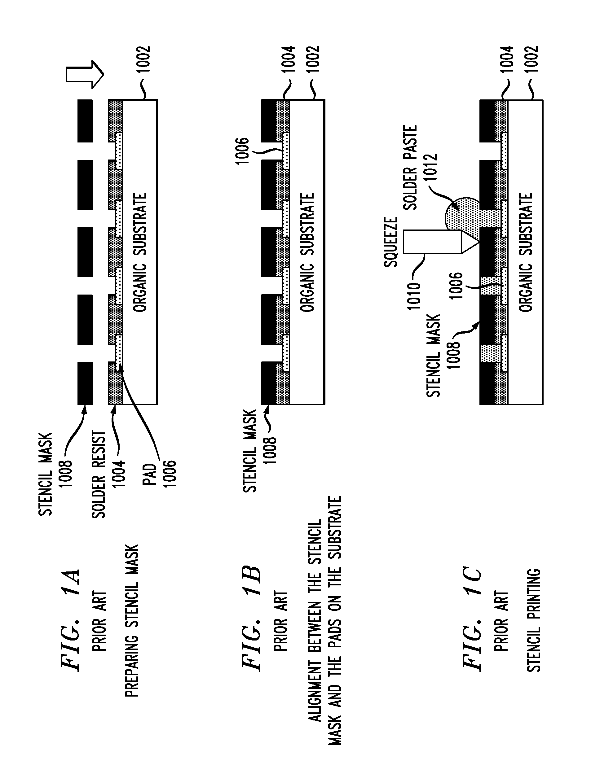
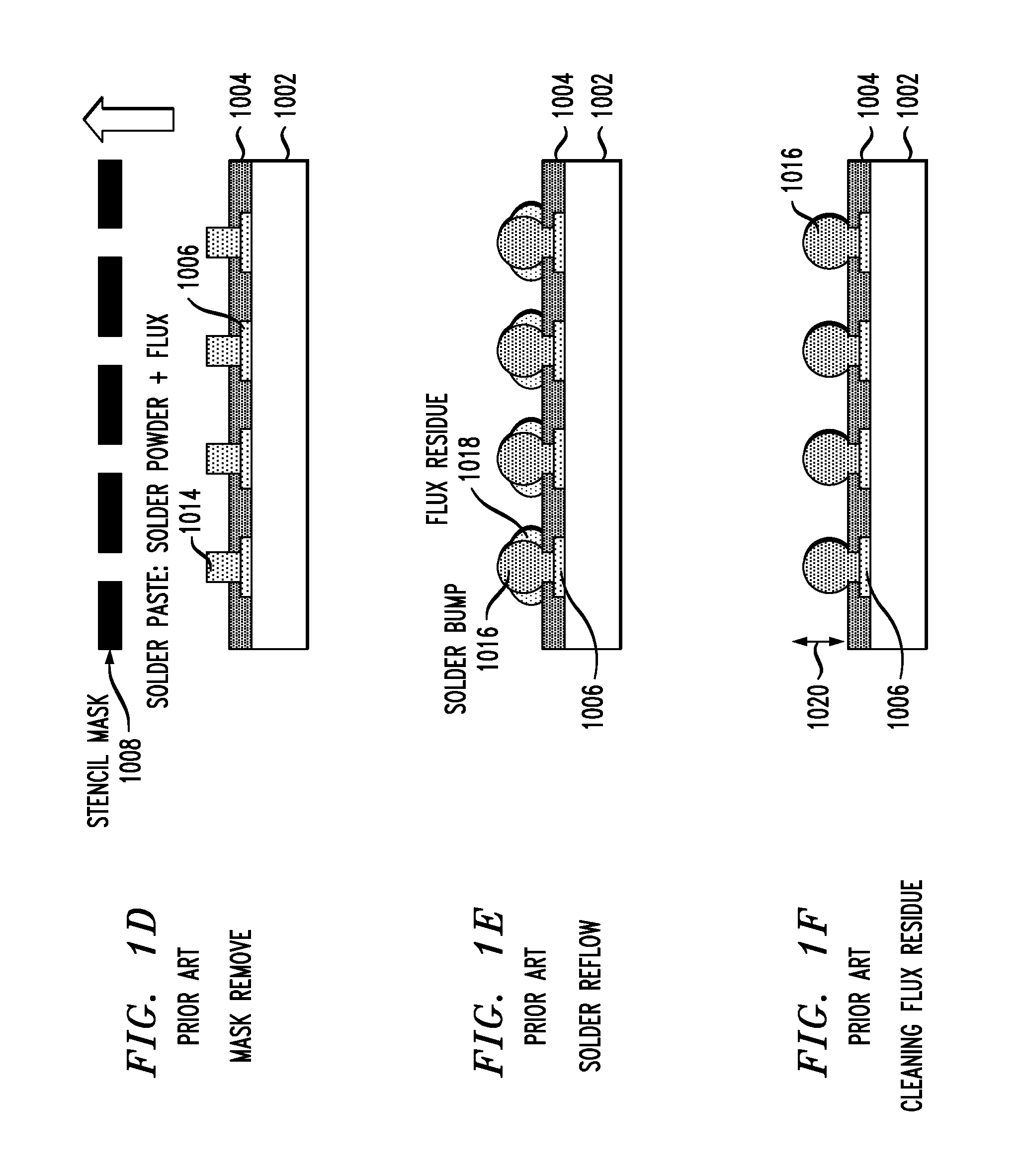
FIELD OF THE INVENTION[0001]The present invention generally relates to the electrical and electronic arts and, more particularly, to injection molded solder techniques, solder mask design methods, and solder deposition on substrates.BACKGROUND OF THE INVENTION[0002]J-W Nah et al., ‘A Study on Coining Processes of Solder Bumps on Organic Substrates,’ IEEE Transactions on electronics packaging manufacturing, Vol. 26, No. 2, April 2003, p. 166, shows a current high volume manufacturing method of forming solder bumps on laminates. The solder paste stencil printing method has been used for forming solder bumps on organic substrates for a long time. As seen in FIGS. 1A and 1B, an organic substrate 1002 is provided with a plurality of pads 1006 and a solder resist layer 1004. A stencil mask 1008 is aligned therewith. As in FIG. 1C, solder paste 1012 is dispensed through the holes in mask 1008 using a squeeze knife or blade 1010. The mask is removed as in FIG. 1D leaving upstanding solder p...

Claims


Application Information

Patent Timeline
Patent Type & Authority Patents(United States)
IPC IPC(8): H01L21/44
CPCH01L21/4853H01L23/49811H01L23/49816H01L24/11H01L24/742H05K3/3452H05K3/3478H01L2224/0401H01L24/05H01L24/13H01L2224/05647H01L2224/10145H01L2224/1131H01L2224/11472H01L2224/1148H01L2224/11849H01L2224/13021H01L2224/13022H01L2224/131H01L2224/1403H01L2224/742H01L2924/01013H01L2924/01029H01L2924/01038H01L2924/01079H01L2924/01082H05K2201/09036H05K2201/09827H05K2201/09845H05K2203/0126H05K2203/043H05K2203/0557H05K2203/0594H01L23/3157H01L2924/014H01L2924/01322H01L2924/01087H01L2924/01005H01L2924/01006H01L2924/01033H01L2924/01042H01L2924/01074H01L2924/01075H01L2924/00014H01L2924/14H05K3/3468H01L2924/00H01L2924/00012
Inventor GRUBER, PETER A.LAURO, PAUL A.NAH, JAE-WOONG
Owner GLOBALFOUNDRIES U S INC
Learn More