
Photomask

a technology of resist masks and masks, applied in the field of photomasks, can solve the problems of inability to remove roundness and difficulty in preventing the corner portion of resist masks from being rounded, and achieve the effect of reducing the roundness of a corner portion of a resist mask, and reducing the roundness of a corner portion

Active Publication Date: 2013-08-20
SEMICON ENERGY LAB CO LTD
View PDF12 Cites 1 Cited by
  • Summary
  • Abstract
  • Description
  • Claims
  • Application Information

AI Technical Summary

Benefits of technology

[0012]However, it is difficult to prevent the corner portion of the resist mask from being rounded even by providing a rectangular auxiliary pattern at the corner portion of the light-blocking portion of the photomask, and therefore roundness cannot be removed. In view of the above, one embodiment of the present invention provides a photomask with which the roundness of a corner portion of a resist mask can be reduced in a photolithography step. Further, one embodiment of the present invention provides a method for manufacturing a semiconductor device with less variation.
[0019]When the auxiliary pattern is provided at the corner portion of the light-blocking portion of the photomask, the intensity of light can be made uniform at the corner portion owing to an optical proximity effect, and the intensity of light projected on a resist through the photomask can be made uniform at the corner portion of the light-blocking portion of the photomask. In a mask which is formed by exposure to the light, the roundness of a corner portion is reduced. Therefore, by etching with the use of the mask, a film pattern having a predetermined shape in which the roundness of a corner portion is reduced can be formed.
[0020]According to one embodiment of the present invention, the roundness of a corner portion of a resist mask can be reduced in a photolithography step. Further, the roundness of a corner portion of a film pattern having a predetermined shape can be reduced. According to one embodiment of the present invention, a method for manufacturing a semiconductor device with less variation can be provided.

Problems solved by technology

However, it is difficult to prevent the corner portion of the resist mask from being rounded even by providing a rectangular auxiliary pattern at the corner portion of the light-blocking portion of the photomask, and therefore roundness cannot be removed.

Method used


Image

  • Photomask
  • Photomask
  • Photomask

Examples


embodiment 1

(Embodiment 1)

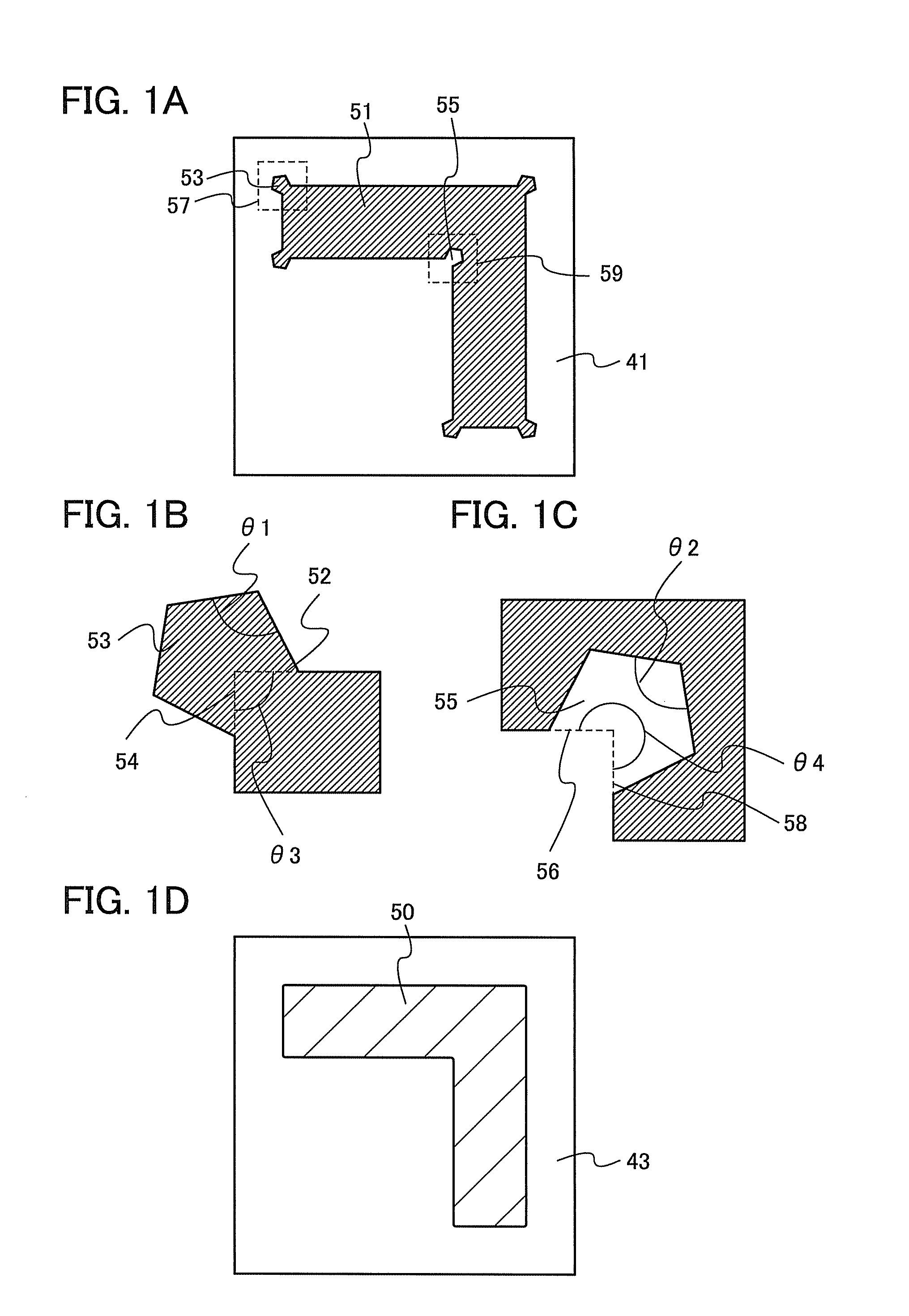
[0032]In this embodiment, the shape of a photomask with which the roundness of a corner portion of a resist mask can be reduced will be described with reference to FIGS. 1A to 1D.

[0033]FIG. 1A is a top view of a photomask including a light-blocking portion 51 over the light-transmitting substrate 41. Auxiliary patterns 53 and 55 are provided at respective corner portions of the light-blocking portion 51.

[0034]For the light-transmitting substrate 41, quartz or the like is used.

[0035]The light-blocking portion 51 is formed using a member which blocks irradiation light in light exposure. Typically, the light-blocking portion 51 is formed using chromium, chromium oxide, or the like.

[0036]Note that in the case where the photomask is a metal mask, the photomask does not necessarily include the light-transmitting substrate 41 and may include only the light-blocking portion 51.

[0037]The auxiliary patterns 53 and 55 each have a shape in which (k+1) sides (k is a natural number ...

embodiment 2

(Embodiment 2)

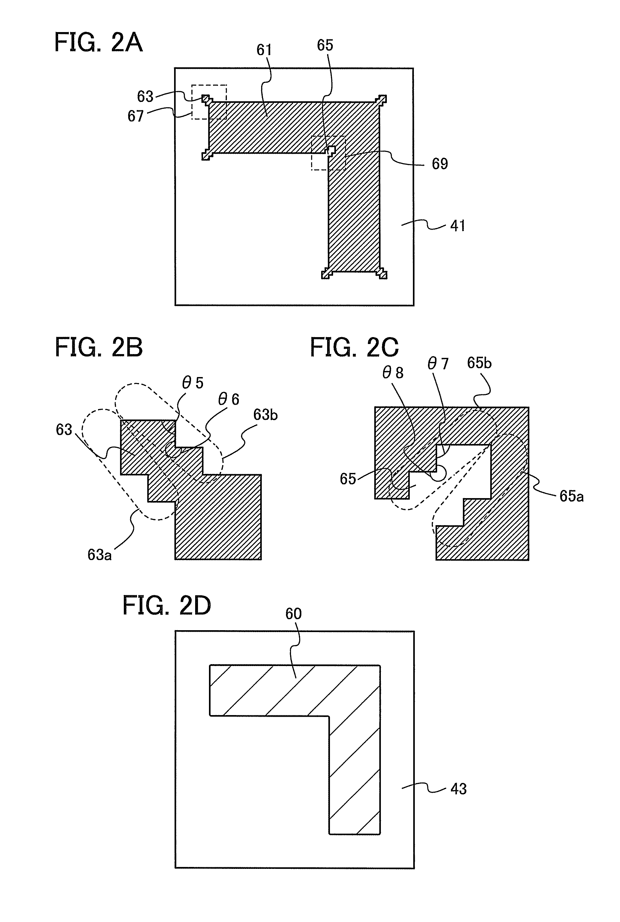
[0052]In this embodiment, a photomask which includes an auxiliary pattern including a zigzag curve will be described with reference to FIGS. 2A to 2D.

[0053]FIG. 2A is a top view of a photomask including a light-blocking portion 61 over the light-transmitting substrate 41. Auxiliary patterns 63 and 65 are provided at respective corner portions of the light-blocking portion 61.

[0054]The light-blocking portion 61 can be formed using a member similar to that of the light-blocking portion 51 described in Embodiment 1.

[0055]Note that in the case where the photomask is a metal mask, the photomask does not necessarily include the light-transmitting substrate 41 and may include only the light-blocking portion 61.

[0056]The auxiliary patterns 63 and 65 each have a shape in which x curves (x is a natural number of 2 or more) each including 2l sides (l is a natural number of 2 or more) alternately forming l corners each having a first angle (greater than 0° and less than 180°) and ...

embodiment 3

(Embodiment 3)

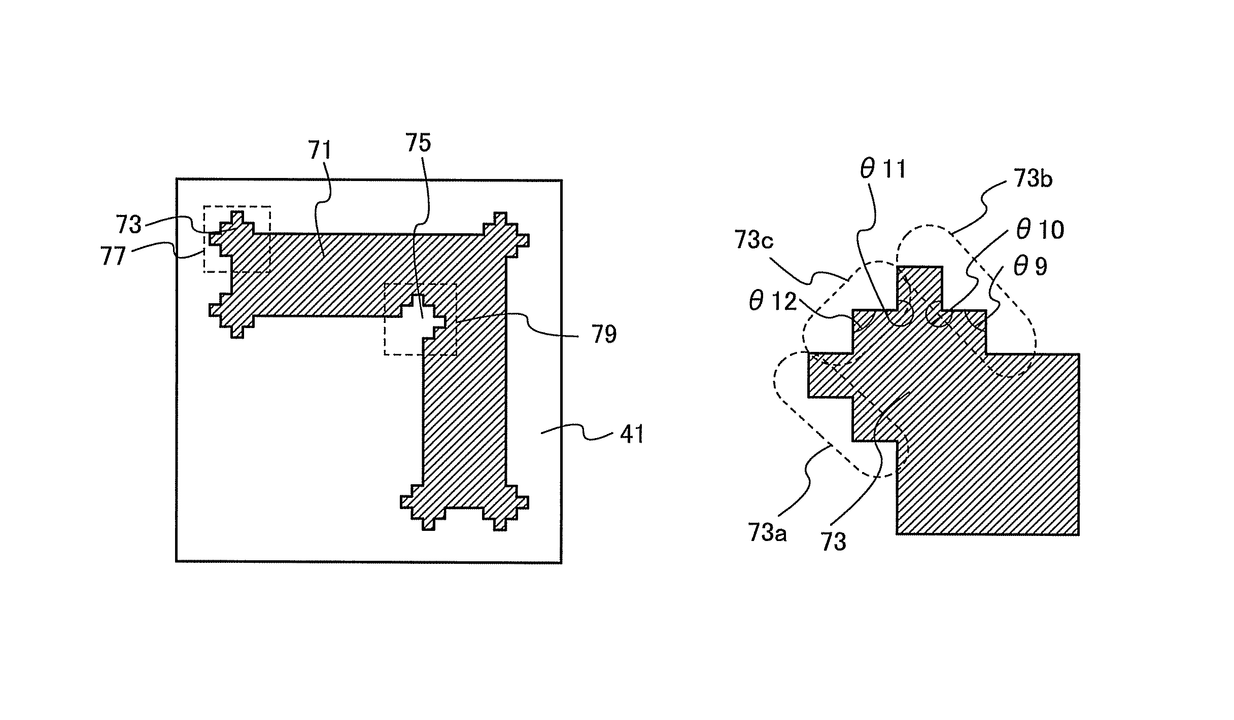
[0073]In this embodiment, another example of a photomask which includes an auxiliary pattern including a zigzag curve will be described with reference to FIGS. 3A to 3D.

[0074]FIG. 3A is a top view of a photomask including a light-blocking portion 71 over the light-transmitting substrate 41. Auxiliary patterns 73 and 75 are provided at respective corner portions of the light-blocking portion 71.

[0075]The light-blocking portion 71 can be formed using a member similar to that of the light-blocking portion 51 described in Embodiment 1.

[0076]Note that in the case where the photomask is a metal mask, the photomask does not necessarily include the light-transmitting substrate 41 and may include only the light-blocking portion 71.

[0077]The auxiliary patterns 73 and 75 each have a shape in which y first curves (y is a natural number of 2 or more) and z second curves (z is a natural number of 1 or more) are connected to each other. The second curve is provided between the first ...


PUM

PropertyMeasurementUnit
angleaaaaaaaaaa
angleaaaaaaaaaa
angleaaaaaaaaaa

Abstract

A photomask is provided, with which the roundness of a corner portion of a resist mask can be reduced in a photolithography step. Further, a method for manufacturing a semiconductor device with less variation is provided. A photomask includes an auxiliary pattern at a corner portion of a light-blocking portion, and (k+1) sides (k is a natural number of 3 or more) form k obtuse angles in the auxiliary pattern. Alternatively, a photomask includes an auxiliary pattern at a corner portion of a light-blocking portion, and the auxiliary pattern includes a zigzag curve.

Description

BACKGROUND OF THE INVENTION[0001]1. Field of the Invention[0002]The present invention relates to a photomask and a method for manufacturing a semiconductor device using the photomask.[0003]2. Description of the Related Art[0004]A field-effect transistor is used as a switching element for controlling a potential of a pixel electrode of a display device typified by a liquid crystal display device and a light-emitting display device. A channel region and a wiring of the field-effect transistor are formed by etching of a semiconductor layer and a conductive layer, respectively, with the use of a resist mask formed by a photolithography step using a photomask.[0005]Owing to high integration of a semiconductor device, light-blocking portions of a photomask are densely arranged. In the photolithography step using the photomask, there is a problem in that the shape of a corner portion of the resist mask is distorted by an optical proximity effect to become different from the shape of the ph...

Claims


Application Information

Patent Timeline
Patent Type & Authority Patents(United States)
IPC IPC(8): G03F1/26G03F1/36G03F1/68
CPCG03F1/144G03F1/36
Inventor SHISHIDO, HIDEAKIYAKUBO, YUTOOISHI, HIROTADA
Owner SEMICON ENERGY LAB CO LTD
Learn More