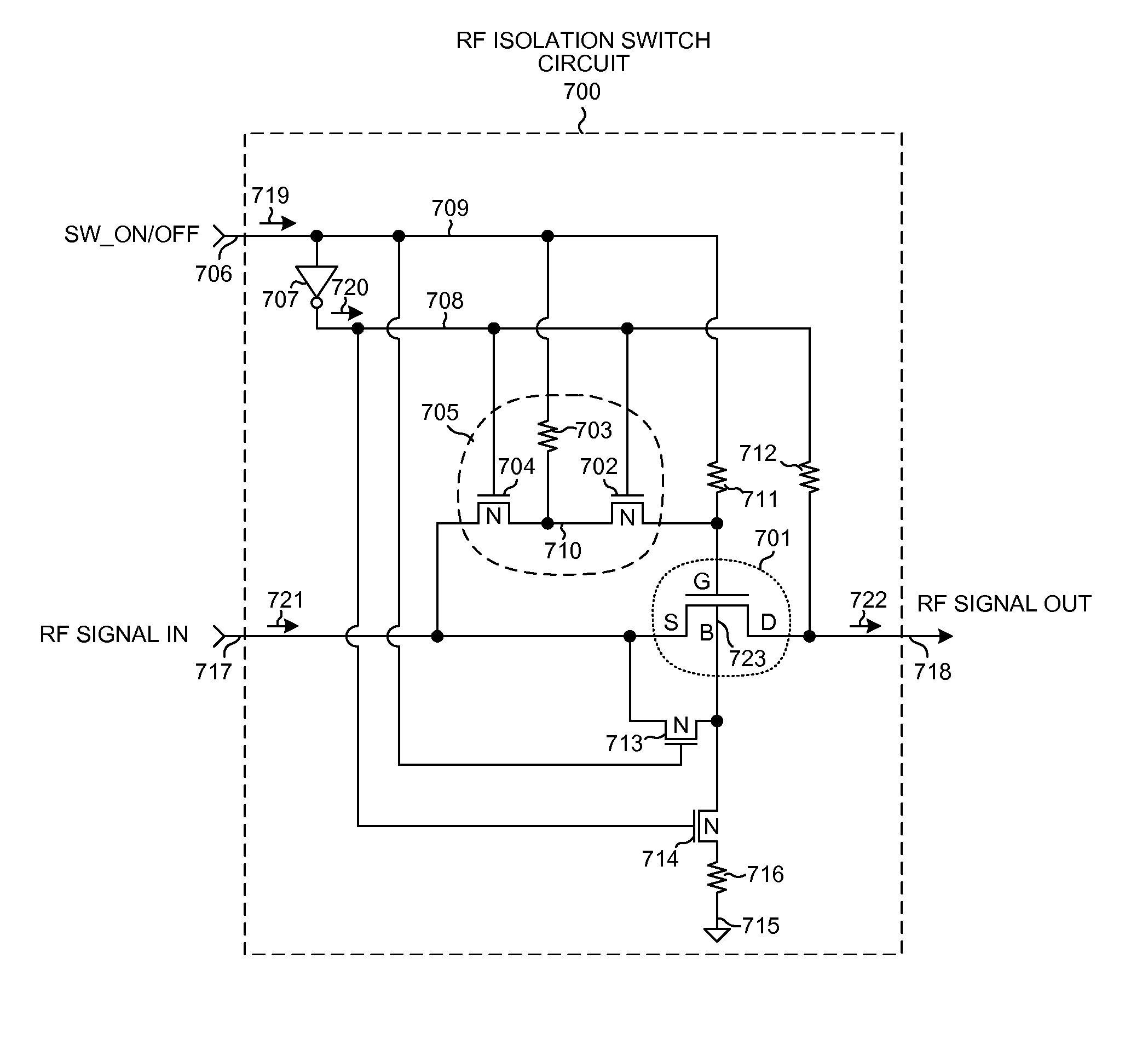
RF isolation switch circuit
a technology of isolation switch and switch circuit, which is applied in the direction of electronic switching, waveguide type devices, pulse techniques, etc., can solve problems such as degrading circuit linearity, and achieve the effect of reducing the threshold voltage of the main transistor and reducing the source-to-drain resistan
- Summary
- Abstract
- Description
- Claims
- Application Information
AI Technical Summary
Benefits of technology
Problems solved by technology
Method used
Image

Examples
Embodiment Construction
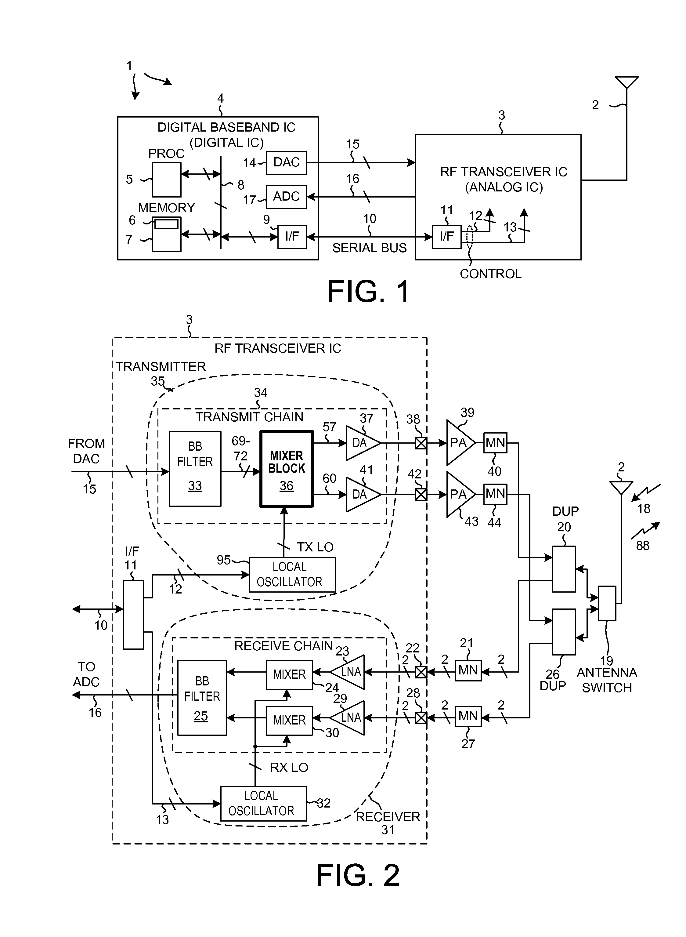
[0034]FIG. 1 is a diagram of a mobile communication device 1 that includes an RF isolation switch circuit in accordance with a first aspect. In this example, mobile communication device 1 is a multi-band cellular telephone handset. Device 1 includes (among other parts not illustrated) an antenna 2 usable for receiving and transmitting cellular telephone communications, an RF (Radio Frequency) transceiver integrated circuit 3, and a digital baseband processor integrated circuit 4. In some examples, the transceiver circuitry and the digital baseband circuitry are implemented on the same integrated circuit, but a two integrated circuit implementation is set forth here for illustration purposes.
[0035]Digital baseband integrated circuit 4 includes a processor 5 that executes a program 6 of processor-executable instructions. Program 6 is stored in a processor-readable medium 7 that in this case is a semiconductor memory. Processor 5 accesses memory 7 via local bus 8. Processor 5 interacts...
PUM
 Abstract
Description
Claims
Application Information
 - R&D
- Intellectual Property
- Life Sciences
- Materials
- Tech Scout
- Unparalleled Data Quality
- Higher Quality Content
- 60% Fewer Hallucinations
Browse by: Latest US Patents, China's latest patents, Technical Efficacy Thesaurus, Application Domain, Technology Topic, Popular Technical Reports.
© 2025 PatSnap. All rights reserved.Legal|Privacy policy|Modern Slavery Act Transparency Statement|Sitemap|About US| Contact US: help@patsnap.com