Optimization of circuits having repeatable circuit instances

a repeatable circuit and circuit technology, applied in the field of electronic, computer arts, can solve the problem that the overall ic yield may fall below an acceptable valu

Inactive Publication Date: 2013-08-20
LSI CORP +1
View PDF13 Cites 106 Cited by
  • Summary
  • Abstract
  • Description
  • Claims
  • Application Information

AI Technical Summary

Benefits of technology

[0004]Illustrative embodiments of the present invention provide methods and apparatus for optimizing a trade-off between IC manufacturing yield and performance (e.g., speed, power, etc.) of compiled memory. Embodiments of the invention provide, for example, techniques for more optimally designing a memory instance by taking into consideration the total number of memory instances, or related circuitry, within the IC comprising the memory instance. In this manner, individual memory instances in the IC can be beneficially designed so that the composite yield of the IC and / or one or more functional characteristics of the IC meet prescribed specifications without significantly compromising the performance of the individual memory instances.
[0006]In accordance with another aspect of the invention, an apparatus is adapted to form a first electronic circuit including a plurality of instances of a repeatable circuit element. The apparatus includes memory and at least one processor coupled to the memory. The processor is operative: (i) to receive a total number of instances of the repeatable circuit element in a design of an integrated circuit including the first electronic circuit and at least a second electronic circuit; and (ii) to configure at least one functional parameter of the first electronic circuit as a function of the total number of instances of the repeatable circuit element in the design of the integrated circuit to thereby satisfy at least a prescribed minimum composite manufacturing yield of the integrated circuit and / or at least one specification of the integrated circuit under prescribed operating conditions.
[0008]Advantages of the invention include, but are not limited to, optimizing overall or composite yield of an IC including a plurality of circuit instances by considering, while forming or designing the IC, a total number of circuit instances within the IC. For ICs with a large amount of memory circuits distributed across a plurality of memory circuit instances, for example, IC yield can be significantly improved compared to memory circuits compiled, designed or formed using standard approaches.

Problems solved by technology

Thus, while individual memory instances may be designed to have a yield high enough to meet prescribed performance specifications, overall IC yield may fall below an acceptable value due, at least in part, to the large number of memory instances, the total number of memory cells and / or the total number of other memory circuits in the IC, which is undesirable.

Method used


Image

  • Optimization of circuits having repeatable circuit instances
  • Optimization of circuits having repeatable circuit instances
  • Optimization of circuits having repeatable circuit instances

Examples


Embodiment Construction

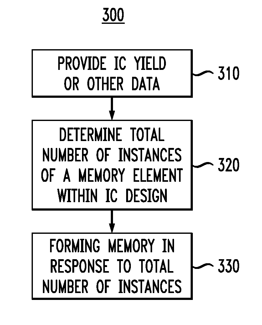
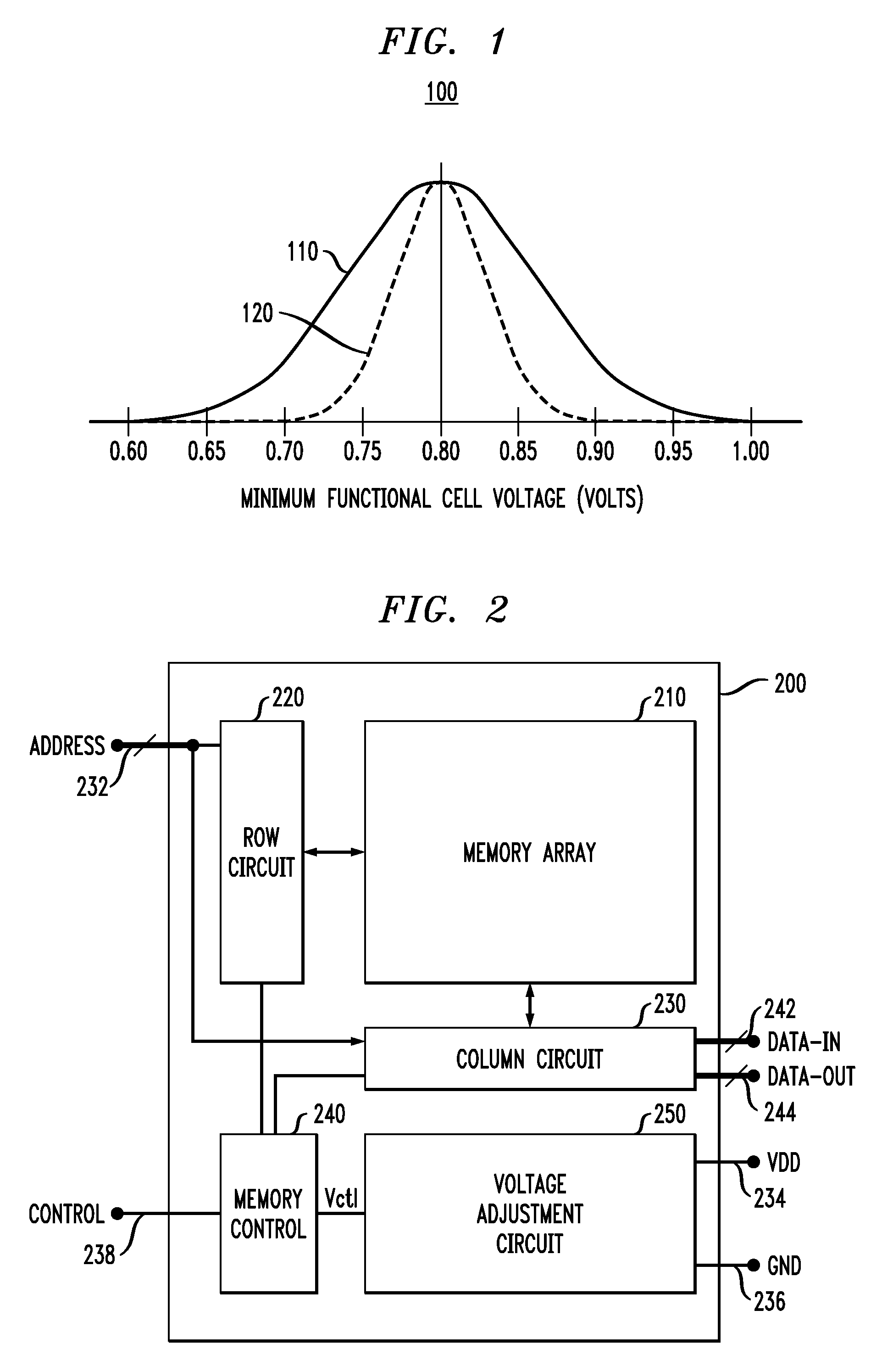
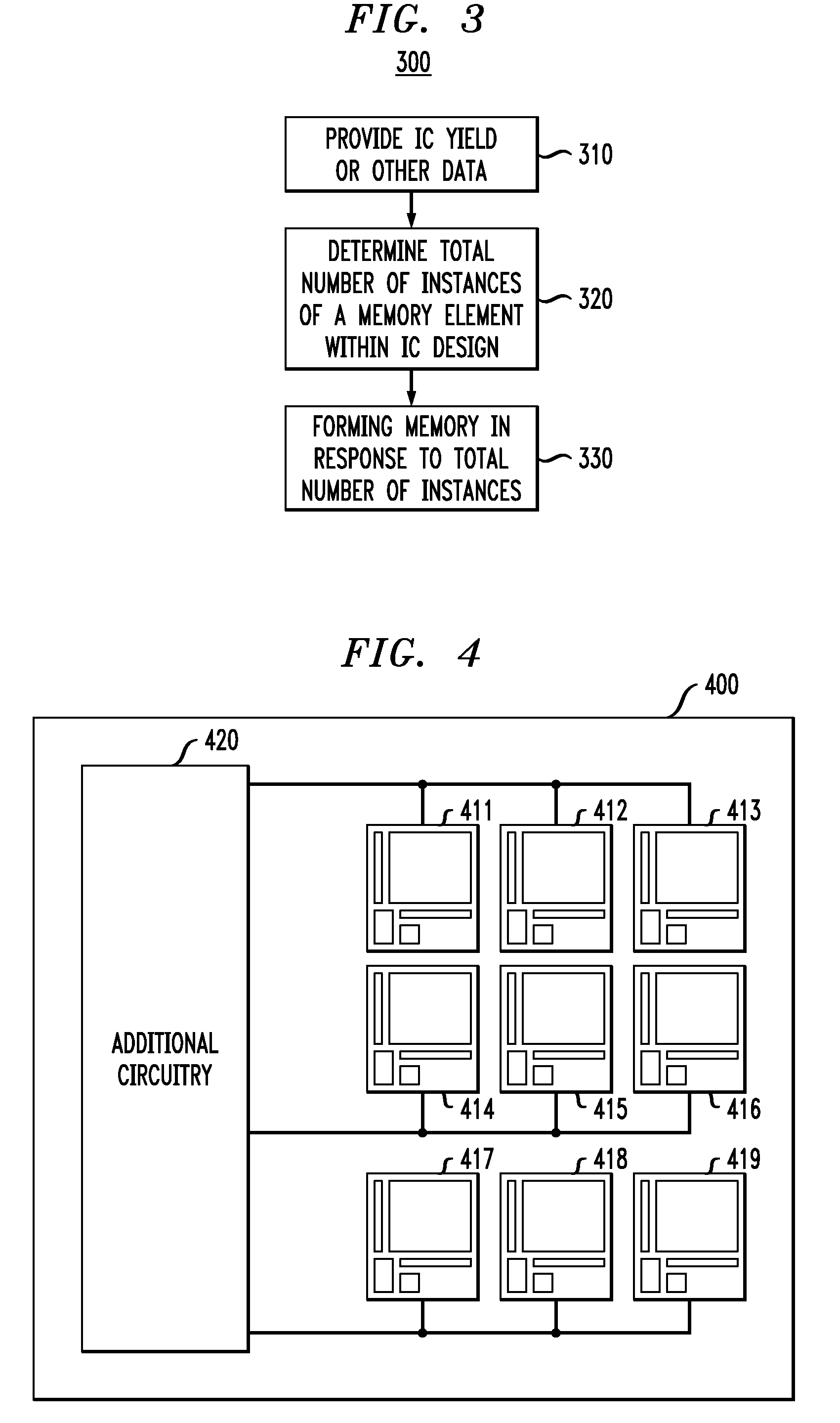
[0018]The present invention will be described herein in the context of illustrative memory circuits and a method for forming a memory circuit. It is to be appreciated, however, that the techniques of the present invention are not limited to the specific circuits and method shown and described herein. Rather, embodiments of the invention are directed broadly to techniques for improving IC manufacturing yield by optimizing a repeatable circuit instance used in an IC design to take into account the number of circuit instances in the IC. For this reason, numerous modifications can be made to the embodiments shown that are within the scope of the present invention. Moreover, although preferred embodiments of the invention are preferably fabricated in a silicon wafer, embodiments of the invention can alternatively be fabricated in wafers comprising other materials, including but not limited to Gallium Arsenide (GaAs), Indium Phosphide (InP), etc. No limitations with respect to the specifi...


PUM


Abstract

Techniques for forming a first electronic circuit including a plurality of instances of a repeatable circuit element include the steps of: obtaining a total number of instances of the repeatable circuit element in a design of an IC including the first electronic circuit and at least a second electronic circuit; and configuring at least one functional parameter of the first electronic circuit as a function of the total number of instances of the repeatable circuit element in the IC to thereby satisfy a prescribed minimum composite manufacturing yield of the IC and / or at least one specification of the IC under prescribed operating conditions.

Description

FIELD OF THE INVENTION[0001]The present invention relates generally to the electrical, electronic, and computer arts, and more particularly relates to circuits having repeatable circuit instances.BACKGROUND OF THE INVENTION[0002]Most embedded memory used in modern integrated circuits (ICs) is predominantly compiled memory. Typically, in ICs comprising a large total amount of memory, the memory is distributed over many memory instances. The term “memory instance” may be defined as an independently functioning memory circuit that can be repeatedly placed and connected in an IC design in a manner consistent with a logic cell in a standard cell library. Often, a larger memory is formed using multiple smaller memory instances, such as, for example, 200 megabits (Mb) or more of memory distributed over tens to hundreds of memory instances.[0003]When memory instances in a conventional IC are compiled, each memory instance is compiled without consideration of the total amount of memory in th...

Claims


Application Information

Patent Timeline
Patent Type & Authority Patents(United States)
IPC IPC(8): G06F17/50
CPCG06F17/5068H01L25/0657H01L25/18H01L2225/06513H01L2225/06517H01L2224/16225G06F30/39H01L2924/00011H01L2924/00014H01L2224/0401
Inventor DELL, RICHARD BRUCEKOHLER, ROSS A.MCPARTLAND, RICHARD J.WERNER, WAYNE E.
Owner LSI CORP
Why Eureka
Try Eureka