
High-speed processor core comprising direct processor-to-memory connectivity

a technology of direct processor and processor core, which is applied in the direction of computation using denominational number representation, pulse technique, instruments, etc., can solve the problems of fpga-based architecture, several limitations to the usefulness of fpga-based devices in their commercial off-the-shelf (“cot”) form, and inability to scale or meet the overall data processing speed needed

Active Publication Date: 2013-08-27
PFG IP +1
View PDF14 Cites 22 Cited by
  • Summary
  • Abstract
  • Description
  • Claims
  • Application Information

AI Technical Summary

Benefits of technology

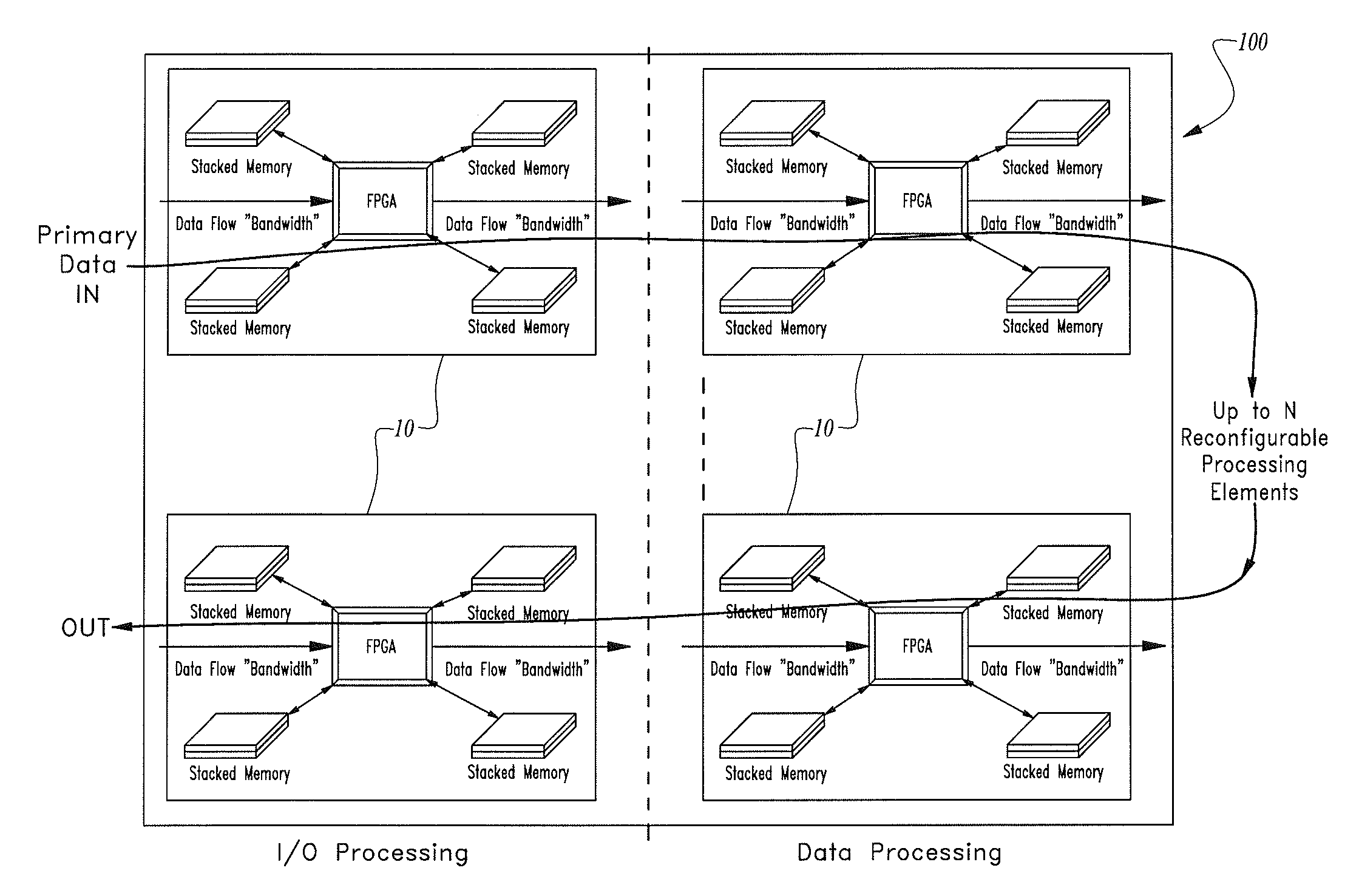
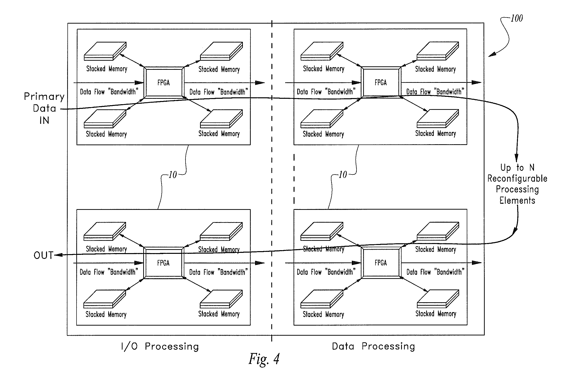
The patent describes a processor core device and architecture that can use three-dimensional memory elements to perform high-speed operations. The device includes two reconfigurable processing elements, each capable of performing a different algorithm. The processing elements can communicate with each other using an access lead network and external memories. The memories can beDDR or QDR SDRAM memories. The architecture can be balanced synchronous or asynchronous, and the processing elements can operate with a variable word width or a word width between 1 to mXN bits. The technical effects of this invention include faster processing, improved performance, and better security for network security algorithms.

Problems solved by technology

Prior art “bused” processor-to-memory structures and architectures in existing processors lack sufficient density of memory and necessary speed of processor-to-memory interconnectivity that is required for the execution of internet attack detection algorithms, internet traffic deep packet inspection algorithms, packet feature extraction and similar algorithm execution at very high line rates (e.g., 100 Gb / s).
Further, prior art “bused memory” architectures lack the ability to scale or to meet overall data processing speeds needed to achieve acceptable results at line rates.
Notwithstanding the great utility of FPGAs, there exist several limitations to the usefulness of these devices in their commercial off the shelf (“COTS”) form.
One constraint with respect to prior art FPGA-based architectures is due to the limited amount of memory available within commercially available FPGAs.
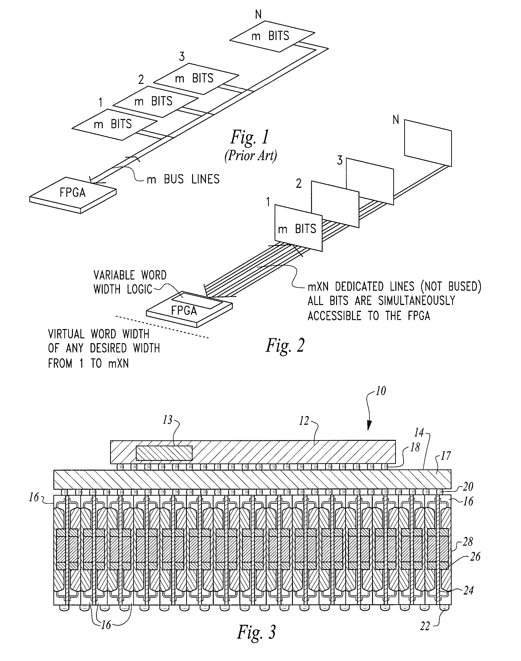
A further limitation of prior art FPGA-based processors is illustrated in FIG. 1 in that FPGAs are typically fabricated based on a design rule that assumes a fixed and limited word width, which design is particularly limiting when the FPGA is used in combination with a large amount of off-device memory such as is required in high performance applications such as data processing or networking.
Yet further, when an FPGA is used to read from and write into a memory array that is arranged in a typical planar (i.e., printed circuit board) fashion, a considerable amount of space on the printed circuit board is required in order to physically provide for the combination of the FPGA and the memory.
Even when space is available for a large planar area to support the FPGA and surrounding memory, relatively long interconnects and buses between the devices inherently increases parasitic impedance problems and timing delays at high processing speeds with associated degradation in system performance.

Method used


Image

  • High-speed processor core comprising direct processor-to-memory connectivity
  • High-speed processor core comprising direct processor-to-memory connectivity
  • High-speed processor core comprising direct processor-to-memory connectivity

Examples


Embodiment Construction

[0041]Turning now to the figures wherein like numerals denote like elements among the several views, FIG. 1 illustrates one of the limitations of prior art FPGA-based processor systems. As earlier stated, FPGAs are generally designed based on one or more design rules that assume a fixed and limited word width which is particularly limiting when used in combination with requisite large amounts of memory in demanding applications such as data processing, deep packet inspection and analysis, cyber-security and networking.

[0042]FIG. 2 is a simplified schematic view of a memory-enhanced field programmable gate array as disclosed in U.S. Pat. No. 6,856,167 entitled “Field Programmable Gate Array with a Variably Wide Word Width Memory” issued Feb. 15, 2005 where all memory bits are simultaneously available to the FPGA such that the FPGA, incorporating suitable logic, can implement a virtual word width of any desired width from 1 to mXN bits. The memory-enhanced field programmable gate arra...


PUM


Abstract

A high-speed processor core having a plurality of individual FPGA-based processing elements configured in a synchronous or asynchronous pipeline architecture with direct processor-to-memory interconnectivity that avoids the latency and bus contention delays of FPGAs using conventional bused memory.The high-speed processor core has one or more memory structures such as SDRAM or QDR electronic memory and is electrically coupled directly to one or more FPGAs using an access lead network to provide a pipelined set of FPGA-based processor elements for processing one or more predetermined operations such as one or more detection algorithms at line rates.

Description

CROSS-REFERENCE TO RELATED APPLICATIONS[0001]This application claims the benefit of U.S. Provisional Patent Application No. 61 / 343,710, filed on May 3, 2010 entitled “High Speed Processing Core Comprising Direct Memory-to-Processor Interconnectivity” pursuant to 35 USC 119, which application is incorporated fully herein by reference.STATEMENT REGARDING FEDERALLY SPONSORED RESEARCH AND DEVELOPMENT[0002]N / ABACKGROUND OF THE INVENTION[0003]1. Field of the Invention[0004]The invention generally relates to the field of high-speed, low latency electronic processors utilizing reconfigurable logic devices such as field programmable gate arrays or “FPGAs”.[0005]More specifically, the invention relates to a high-speed electronic processor core comprising direct processor-to-memory interconnectivity that avoids the latency and bus contention delays of prior art processors incorporating bused memory in connection with an FPGA.[0006]2. Description of the Prior Art[0007]The ability to perform mas...

Claims


Application Information

Patent Timeline
IPC IPC(8): H03K19/173
CPCG06F15/7867H03K19/17776H03K19/17758
Inventor LEON, JOHN
Owner PFG IP
Learn More