High holding voltage BJT clamp with embedded reverse path protection in BCD process

a reverse path protection and high holding voltage technology, applied in the field of esd protection, can solve the problems of the total voltage between two high voltage pins exceeding the parasitic npn turn-on voltage, the risk of irreversible burnout of one or both esd devices, etc., to reduce the risk of irreversible burnout, increase the base contact area of the lateral bjt, and increase the efficiency of the reverse path body diode

Active Publication Date: 2013-09-17
NAT SEMICON CORP
View PDF2 Cites 0 Cited by
  • Summary
  • Abstract
  • Description
  • Claims
  • Application Information

AI Technical Summary

Benefits of technology

[0007]According to the invention there is provided a method of reducing the risk of irreversible burnout due to transient latch-up between two adjacent high voltage pins of a structure in which one pin is protected in the forward direction by a lateral BJT that includes at least one collector finger, at least one emitter finger and a base, and that defines an embedded reverse path body diode, comprising increasing the efficiency of the reverse path body diode by increasing the base-contact area of the lateral BJT. The increasing of the base contact area of the BJT may comprise at least one of forming an enlarged base contact island to the base of the lateral BJT, adding additional base contact islands, and insofar as the structure includes a buried layer of the same doping type as the base of the BJT, adding a sinker epitaxial tie of the same doping type as the base of the BJT that extends down to the buried layer. Insofar as the lateral BJT includes a sinker epitaxial tie the method may further comprise eliminating any base contact islands.

Problems solved by technology

Depending on internal circuit design and metallization routing, the latch-up current through the parasitic NPN can simply pass to ground through the ESD devices, but in many situations the current causes irreversible burnout of one or both ESD devices.
However, if two clamps are placed adjacent to each other with minimum isolation rules, the total voltage between two high voltage pins may exceed the parasitic NPN turn-on voltage, especially in the case of fast transient modes e.g. due to excessive reverse path diode voltage drop.

Method used


Image

  • High holding voltage BJT clamp with embedded reverse path protection in BCD process
  • High holding voltage BJT clamp with embedded reverse path protection in BCD process
  • High holding voltage BJT clamp with embedded reverse path protection in BCD process

Examples


Embodiment Construction

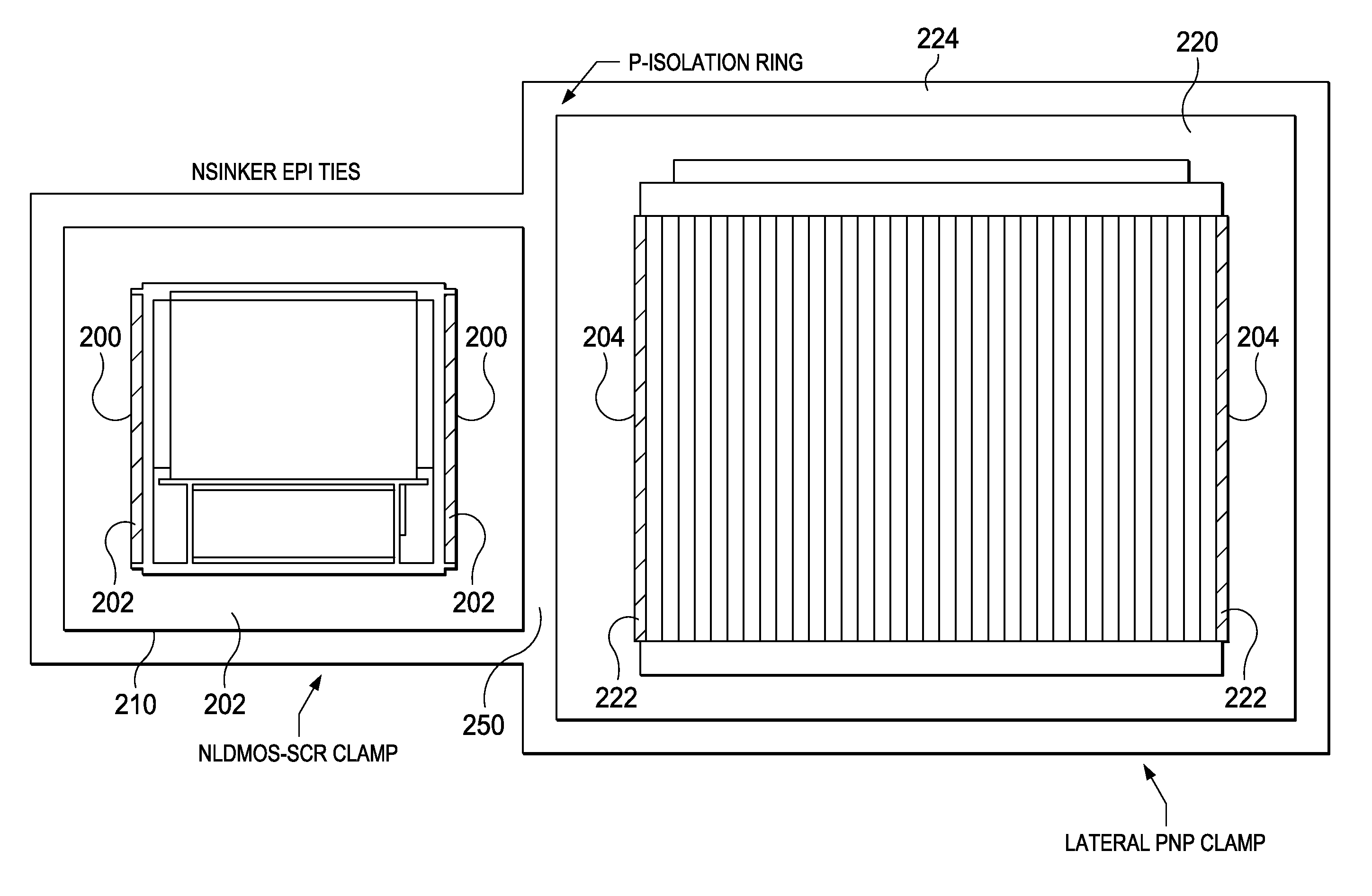
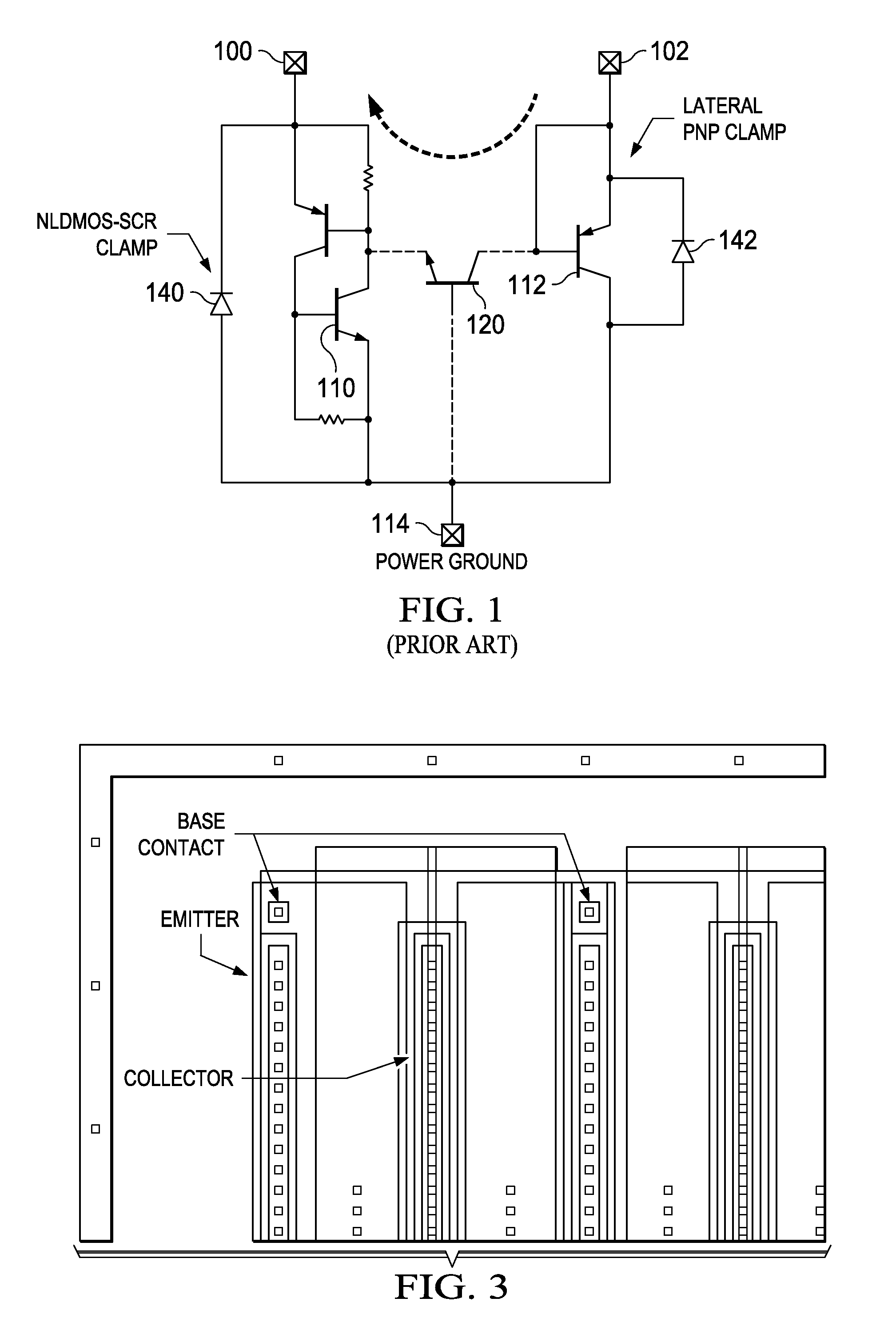
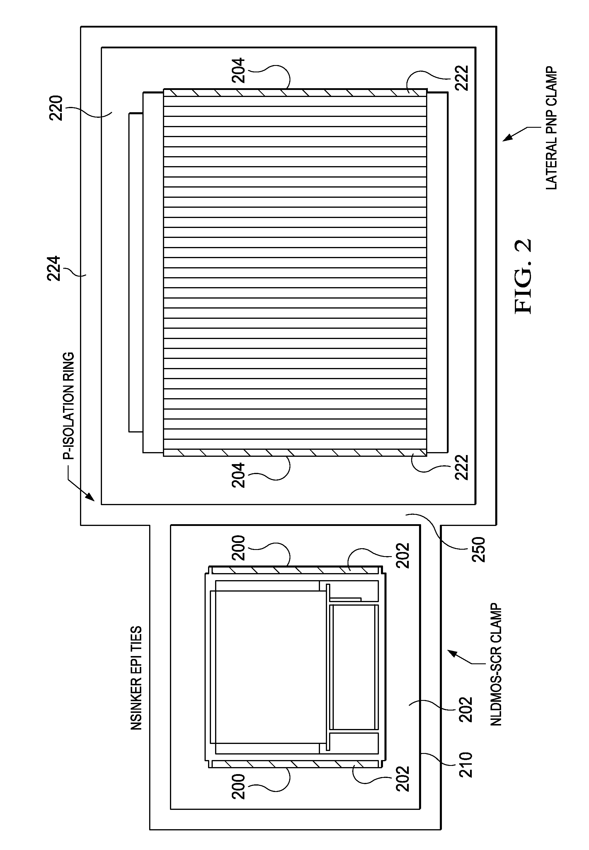
[0018]As mentioned above, if two clamps are placed in close proximity to each other with minimum isolation rules, an alternative current path is produced through the parasitic NPN transistor between them. In the case of a high voltage pin-to-high voltage pin combination the total voltage may exceed the parasitic NPN turn on voltage especially in fast transient mode e.g., due to excessive reverse path diode voltage drop such as the voltage drop across diode 142 in FIG. 1.

[0019]In the case of a lateral BJT clamp such as lateral PNP or lateral NPN clamp implemented in a BCD process technology, or implemented in an extended voltage CMOS process, wherein the circuit defines a parasitic NPN the present invention increases the efficiency of the body diode in the lateral BJT by enlarging the base contact area, or by adding base contacts e.g. two or more base contacts, or by adding at least one sinker epi tie of same doping type as the base of the lateral BJT (n-sinker region that extends do...


PUM


Abstract

In the case of adjacent high voltage nodes in which one node is protected by a lateral BJT clamp, the irreversible burnout due to transient latch-up between the two adjacent high voltage pins of the structure is avoided by increasing the base contact region by including a sinker connected to the base.

Description

FIELD OF THE INVENTION[0001]The invention relates to ESD protection. In particular it relates to n-epi to n-epi lateral latch-up.BACKGROUND OF THE INVENTION[0002]In high voltage processes it is common to have transient latch-up. For example latch-up current may flow between adjacent high voltage pins protected by high voltage electrostatic discharge (ESD) devices or between the ESD device and internal circuitry.[0003]In particular, in structures where there are n and p laterally spaced regions such as n-type epitaxial (n-epi) regions and p-isolation, a parasitic current path can be created through the lateral parasitic NPN formed by the n-epi regions and p-isolation to provide an n-epi to n-epi transient latchup scenario. This is, for instance found in the case of a BCD process between an NLDMOS-SCR ESD clamp and a laterally arranged PNP clamp. The lateral PNP can also be implemented in an extended voltage CMOS process to define the parasitic NPN.[0004]FIG. 1 shows a circuit diagram...

Claims


Application Information

Patent Timeline
Patent Type & Authority Patents(United States)
IPC IPC(8): H01L29/66
CPCH01L27/0259H01L29/735
Inventor VASHCHENKO, VLADISLAV
Owner NAT SEMICON CORP
Why Eureka
Try Eureka