

Substrate treating apparatus with inter-unit buffers
a technology of buffers and substrates, applied in the field of substrate treatment apparatus, can solve the problems of lowering the quality of substrate treatment, the inability of coating blocks to carry out a series of treatments, etc., and achieve the effect of preventing lowering the quality of treatmen
- Summary
- Abstract
- Description
- Claims
- Application Information
AI Technical Summary
Benefits of technology
Problems solved by technology
Method used
Image

Examples
Embodiment Construction
[0081]One embodiment of this invention will be described in detail hereinafter with reference to the drawings.
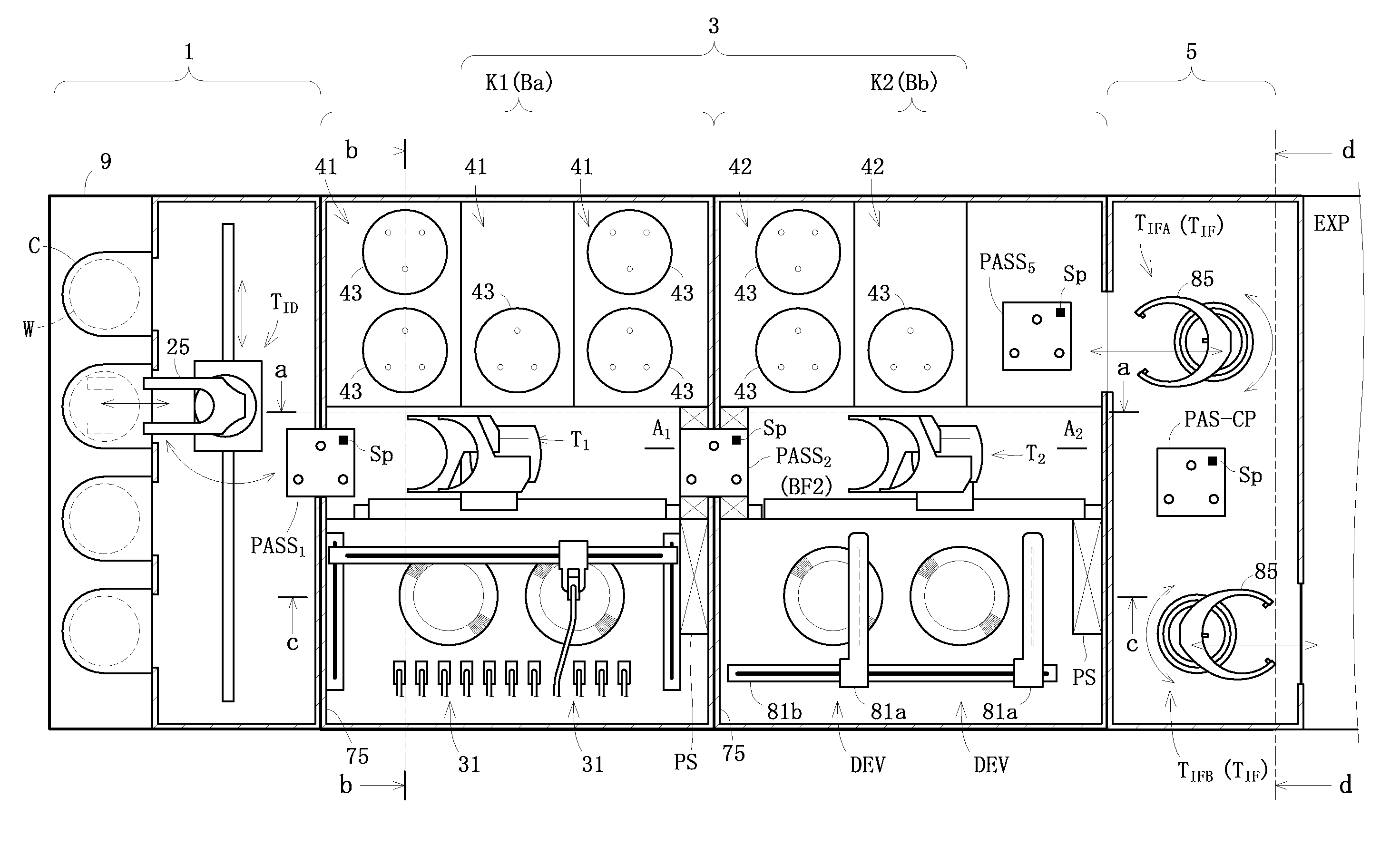
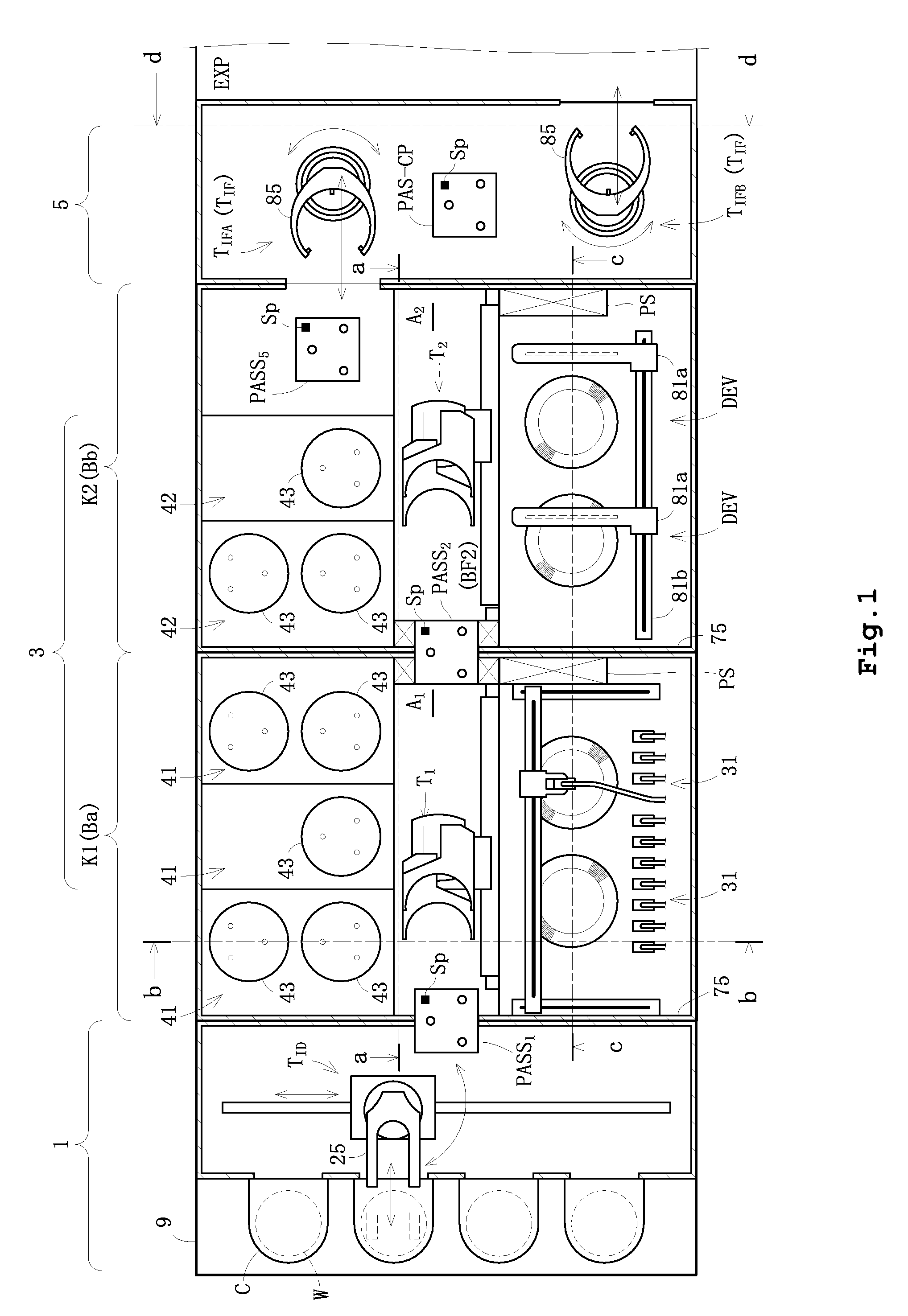
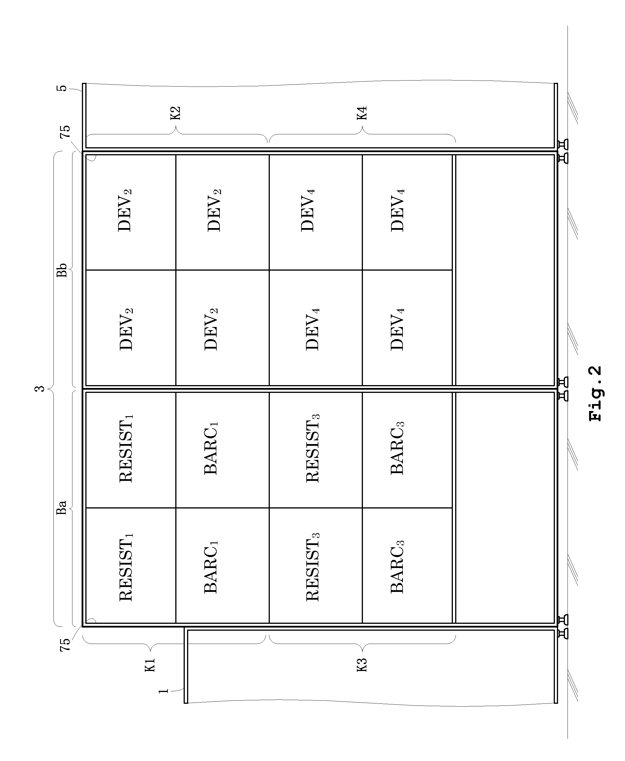
[0082]FIG. 1 is a plan view showing an outline of a substrate treating apparatus according to this embodiment. FIGS. 2 and 3 are schematic side views showing an arrangement of treating units included in the substrate treating apparatus. FIGS. 4 through 7 are views in vertical section taken on lines a-a, b-b, c-c and d-d of FIG. 1, respectively.
[0083]This embodiment provides a substrate treating apparatus for forming resist film or the like on substrates (e.g. semiconductor wafers) W, and developing exposed wafers W. This apparatus is divided into an indexer section (hereinafter called “ID section”) 1, a treating section 3 and an interface section (hereinafter called “IF section”) 5. The ID section 1, treating section 3 and IF section 5 are arranged adjacent one another in the stated order. An exposing machine EXP, which is an external apparatus separate from this apparatus, ...
PUM
 Abstract
Description
Claims
Application Information