Contact architecture for 3D memory array

a contact architecture and memory array technology, applied in semiconductor devices, digital storage, instruments, etc., can solve the problems of increasing the cost of vertical interconnect implementation, reducing yield, and interconnect structures, and achieves high yield manufacturing and low cost.

Active Publication Date: 2013-11-05
MACRONIX INT CO LTD
View PDF28 Cites 11 Cited by
  • Summary
  • Abstract
  • Description
  • Claims
  • Application Information

AI Technical Summary

Benefits of technology

[0011]A vertical interconnect architecture for a three-dimensional (3D) memory device suitable for low cost, high yield manufacturing is described. Conductive lines (e.g. word lines) for the 3D memory array, and contact pads for vertical connectors used for couple the array to decoding circuitry and the like, are formed as parts of the same patterned level of material. The same material layer can be used to form the contact pads and the conductive access lines by an etch process using a single mask. By forming the contact pads concurrently with the conductive lines, the patterned material of the contact pads can protect underlying circuit elements which could otherwise be damaged during patterning of the conductive lines.

Problems solved by technology

One drawback of conventional three-dimensional stacked memory devices is that the vertical interconnect structures to different portions in the array are formed separately in different levels overlying the array.
The cost to implement the vertical interconnects increases with the number of lithographic steps needed.
In addition, issues such as mask alignment and etch selectivity during manufacturing can reduce yield.

Method used


Image

  • Contact architecture for 3D memory array
  • Contact architecture for 3D memory array
  • Contact architecture for 3D memory array

Examples


Embodiment Construction

[0025]A detailed description of embodiments of the present invention is provided with reference to the FIGS. 1-11.

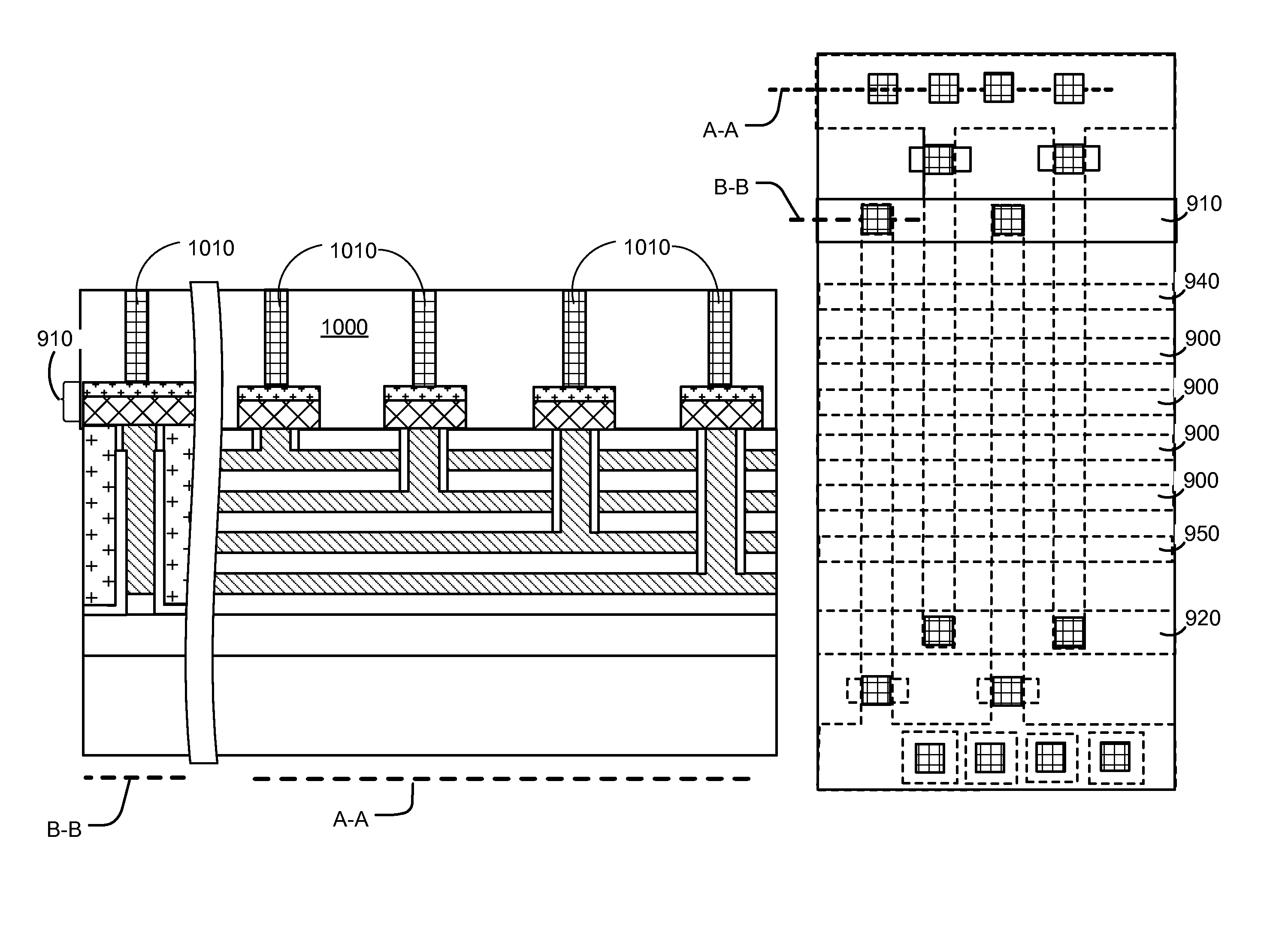
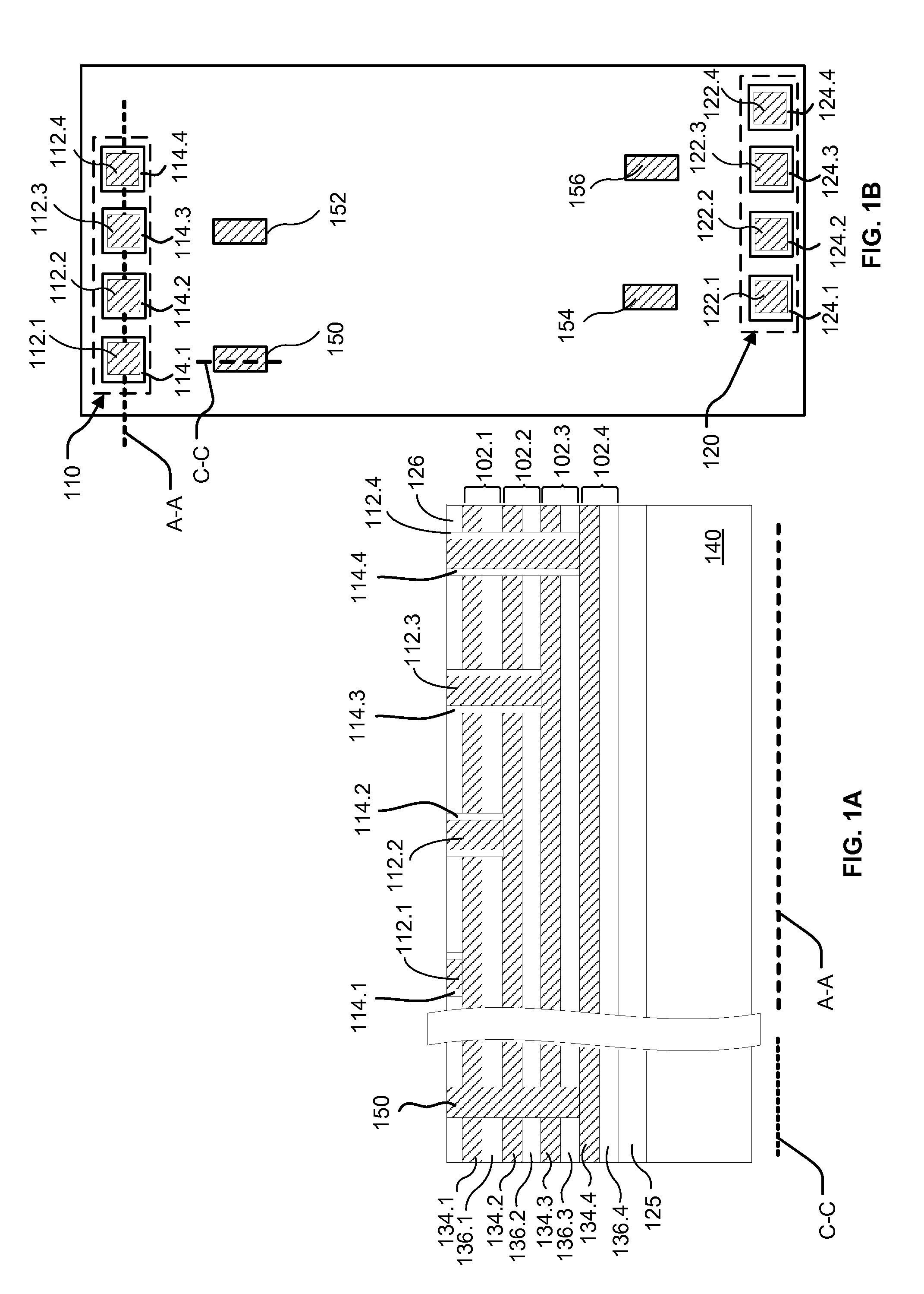
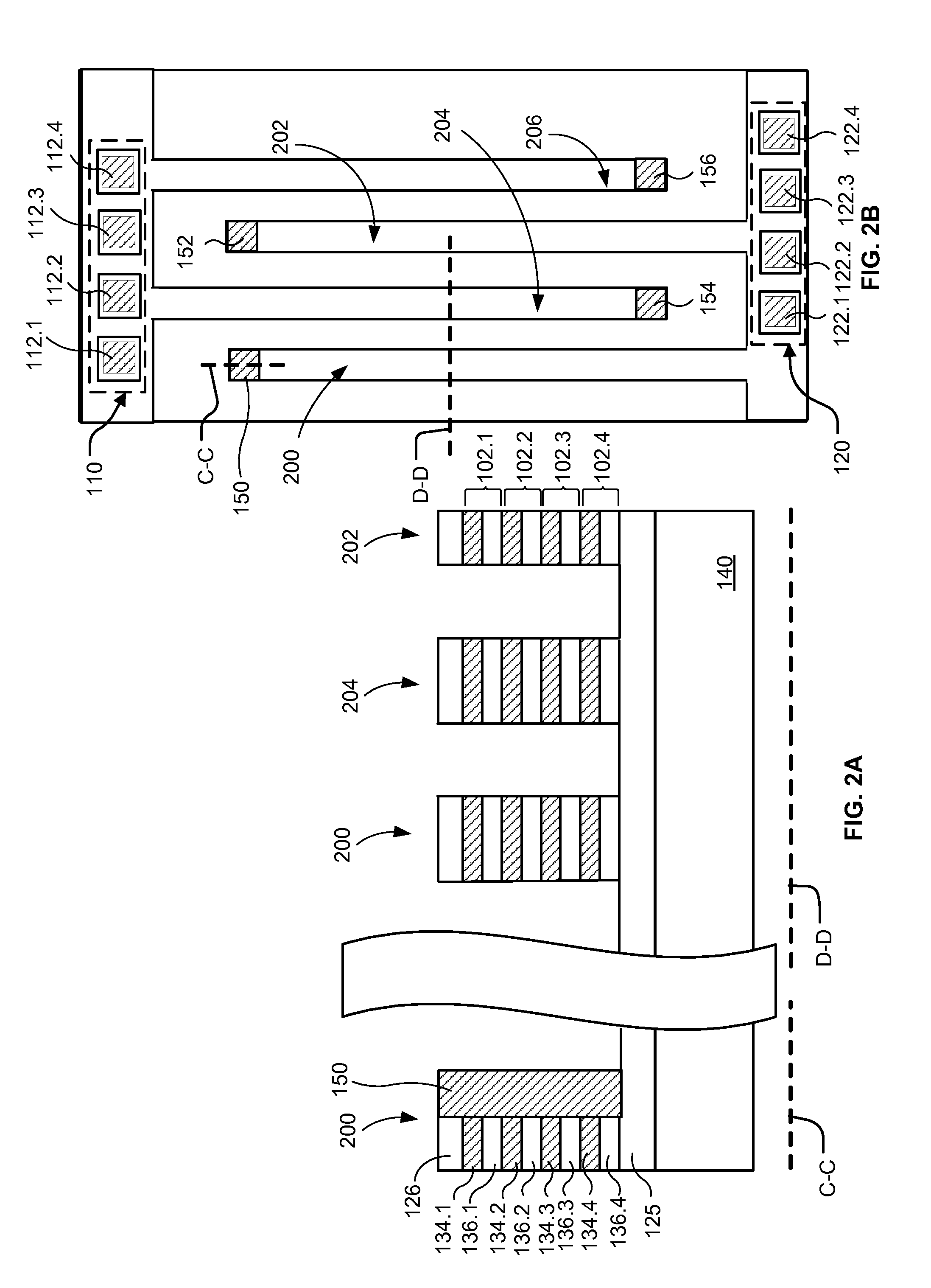
[0026]FIGS. 1A and 1B illustrate cross-sectional and top views of a structure following a first stage in a process for manufacturing a three-dimensional stacked memory device. In this example, four levels 102, labeled 102.1, 102.2, 102.3, 102.4, are illustrated, which is representative of a structure that can include many levels.

[0027]The four levels 102 are separated from an underlying semiconductor substrate 140 by one or more dielectric layers 125. A top dielectric layer 126 overlies the four levels 102.

[0028]The levels 102 include respective layers 134 of conductive material. In the illustrated example, the layers 134 are semiconductor material such as doped polysilicon. The levels 102 also include respective layers 136 of insulating material separating the semiconductor material layers 134 of the different levels 102.

[0029]The structure also includes a first stepped...


PUM


Abstract

A vertical interconnect architecture for a three-dimensional (3D) memory device suitable for low cost, high yield manufacturing is described. Conductive lines (e.g. word lines) for the 3D memory array, and contact pads for vertical connectors used for couple the array to decoding circuitry and the like, are formed as parts of the same patterned level of material. The same material layer can be used to form the contact pads and the conductive access lines by an etch process using a single mask. By forming the contact pads concurrently with the conductive lines, the patterned material of the contact pads can protect underlying circuit elements which could otherwise be damaged during patterning of the conductive lines.

Description

CROSS-REFERENCE TO RELATED APPLICATIONS[0001]This application is related to U.S. patent application Ser. No. 13 / 114,931 filed 24 May 2011, entitled “Multilayer Connection Structure and Making Method,” and to U.S. patent application Ser. No. 13 / 245,587 filed Sep. 26, 2011 entitled “Architecture for a 3-D Memory Array,”.BACKGROUND[0002]1. Field of the Invention[0003]The present invention relates generally to high density integrated circuit devices, and more particularly to interconnect structures for multi-level three-dimensional stacked devices.[0004]2. Description of Related Art[0005]As critical dimensions of devices in integrated circuits shrink to the limits of common memory cell technologies, designers have been looking for techniques for stacking multiple levels of memory cells to achieve greater storage capacity, and to achieve lower costs per bit. For example, thin film transistor techniques are applied to charge trapping memory technologies in Lai, et al., “A Multi-Layer Stac...

Claims


Application Information

Patent Timeline
Patent Type & Authority Patents(United States)
IPC IPC(8): H01L21/336G11C5/06
CPCH01L27/11206H01L27/11519H01L27/11551H01L27/11556H01L27/11565H01L27/11578H01L27/11582H01L27/0688H01L27/10H01L27/2481H10B63/84H10B20/20H10B41/10H10B41/20H10B43/10H10B43/20H10B41/27H10B43/27
Inventor CHEN, SHIH-HUNGSHIH, YEN-HAOLUE, HANG-TING
Owner MACRONIX INT CO LTD
Why Eureka
Try Eureka