Solid-state imaging apparatus, camera, and method of manufacturing solid-state imaging apparatus

a technology of solid-state imaging and imaging apparatus, which is applied in the direction of television system scanning details, radioation control devices, television systems, etc., can solve the problems of difficult reduction of the occupied area of the vertical transfer channel area that functions as a transfer path for signal charge, difficult to reduce the above problems, etc., and achieves the effect of increasing the area of the light-receiving surface per pixel and improving the quality of the captured imag

Inactive Publication Date: 2013-11-26
SONY CORP
View PDF13 Cites 9 Cited by
  • Summary
  • Abstract
  • Description
  • Claims
  • Application Information

AI Technical Summary

Benefits of technology

[0015]Therefore, in the solid-state imaging apparatus, there is a case in which the quality of a captured image is decreased.
[0016]Accordingly, it is desirable to provide a solid-state imaging apparatus capable of increasing the area of a light-receiving surface per pixel and improving the quality of a captured image, a camera, and a method of manufacturing the solid-state imaging apparatus.
[0022]According to the embodiments of the present invention, it is possible to provide a solid-state imaging apparatus, a camera, and a method of manufacturing the solid-state imaging apparatus that are capable of increasing the area of a light-receiving surface per pixel and improving the quality of a captured image.

Problems solved by technology

More specifically, in an image-sensing area, since reduction of an area other than the light-receiving surface is difficult, the reduction of the area of the light-receiving surface often becomes necessary.
As a result, the above problem may occur.
For example, in the image-sensing area, the occupied area of the vertical transfer channel area that functions as a transfer path for signal charge is difficult to reduce for the purpose of securing transfer efficiency and saturation signals.
Furthermore, there is a case in which a light-shielding film is difficult to form into a thin film for the purpose of securing a light-shielding characteristic.
Furthermore, also, regarding an interlayer insulating film between the transfer electrode and the light-shielding film, there is a case in which the interlayer insulating film is difficult to form into a thin film for the purpose of securing an insulating characteristic.
For this reason, it is necessary for the area of the light-receiving surface to be reduced, and a problem of the proportion of sensitive electrons decreasing below the pixel reduction ratio may occur.

Method used


Image

  • Solid-state imaging apparatus, camera, and method of manufacturing solid-state imaging apparatus
  • Solid-state imaging apparatus, camera, and method of manufacturing solid-state imaging apparatus
  • Solid-state imaging apparatus, camera, and method of manufacturing solid-state imaging apparatus

Examples


first embodiment

Apparatus Configuration

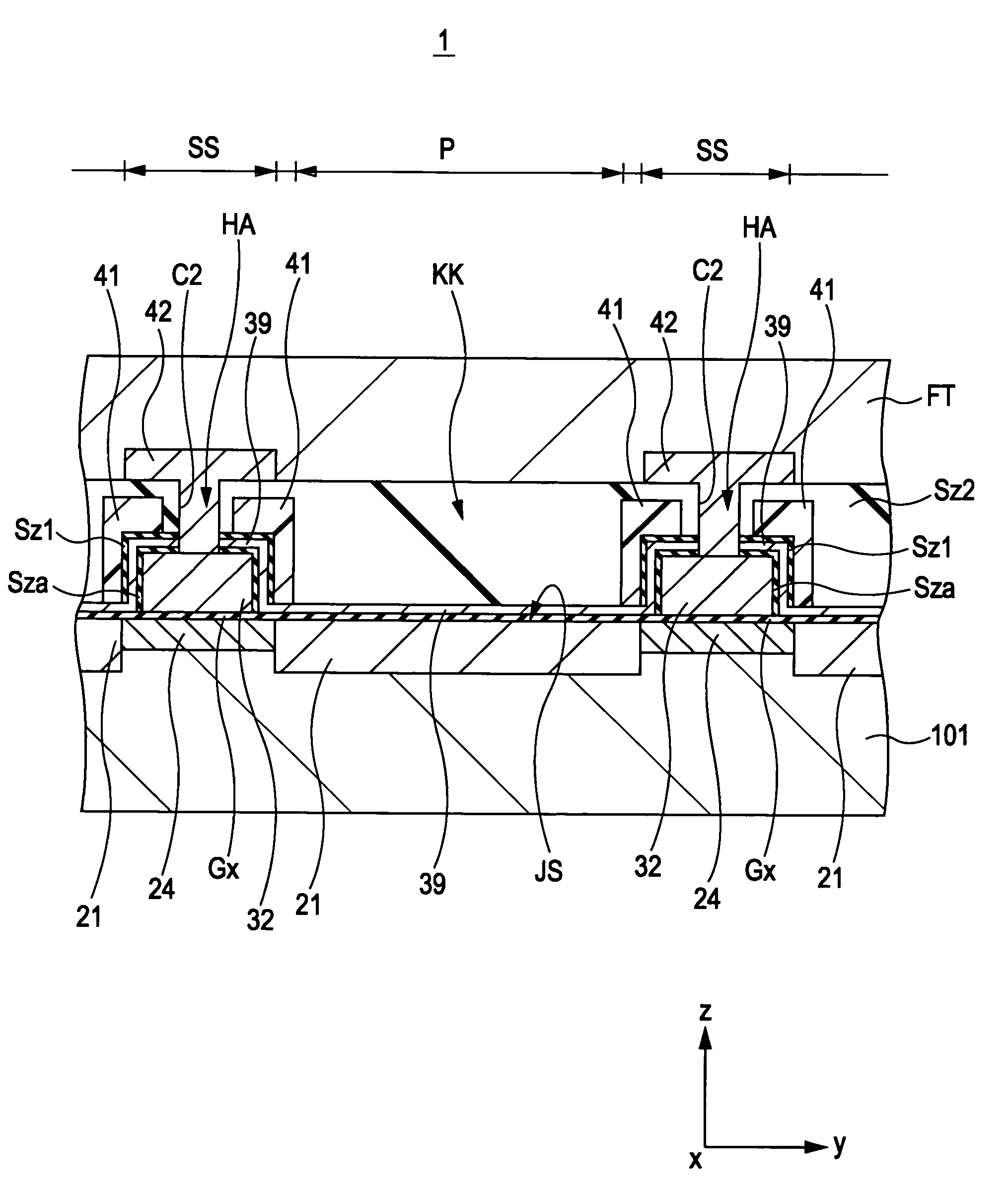
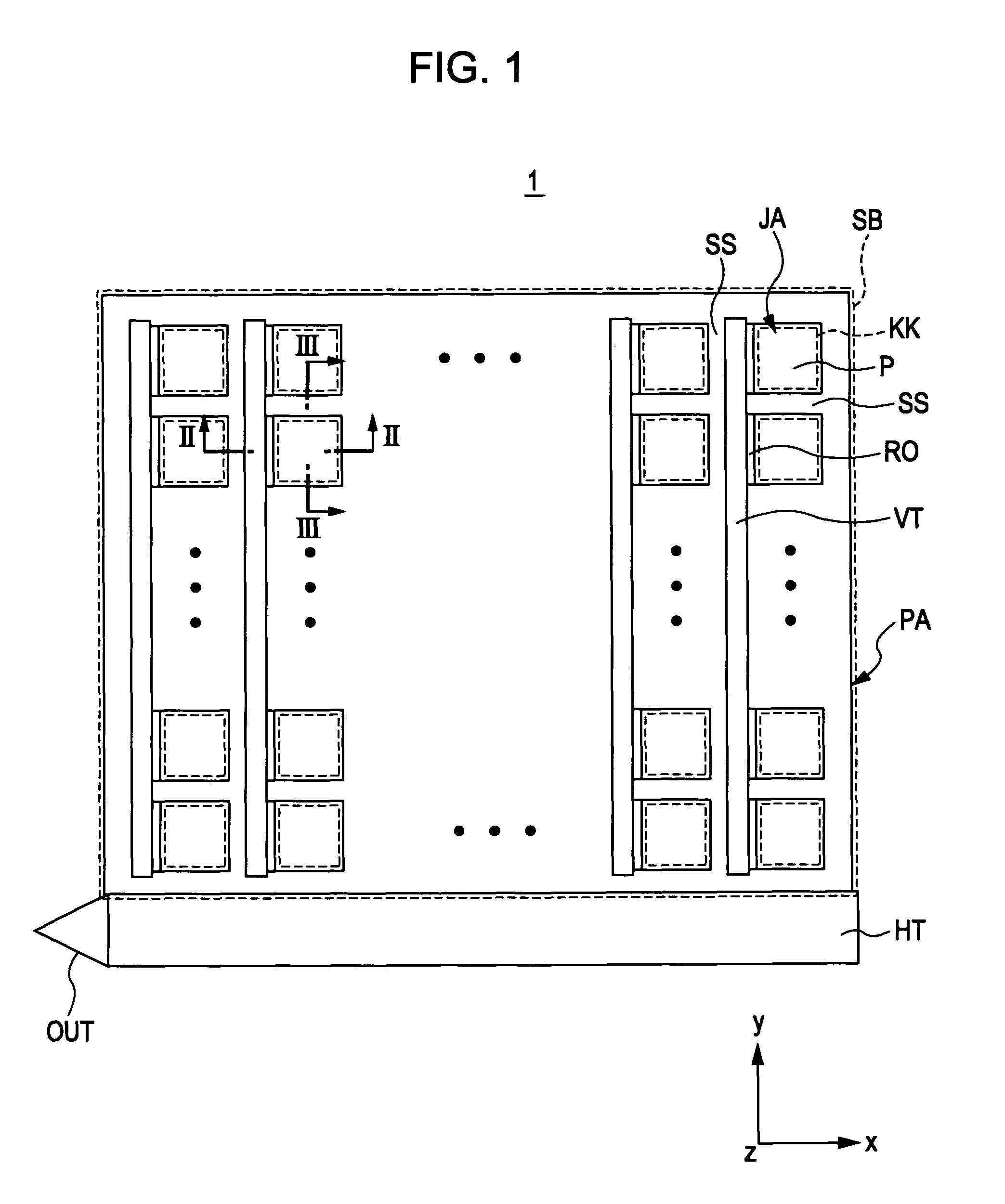
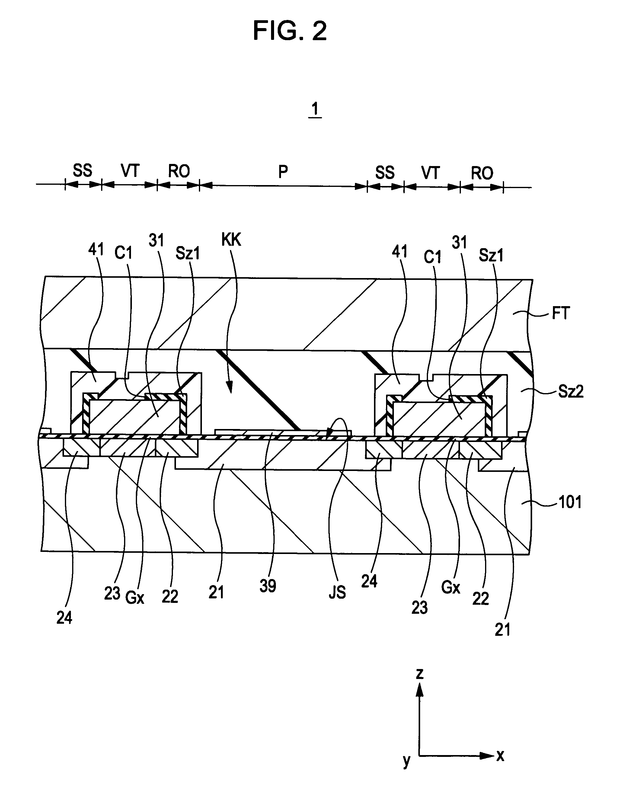
[0051]FIG. 1 is a plan view showing the outline of the entire configuration of a solid-state imaging apparatus 1 according to a first embodiment of the present invention.

[0052]As shown in FIG. 1, the solid-state imaging apparatus 1 is, for example, a CCD image sensor using an interline transfer method, with image capturing being performed in an image-sensing area PA.

[0053]In this image-sensing area PA, as shown in FIG. 1, photoelectric conversion units P, charge reading units RO, vertical transfer register units VT, and a light shielding unit SB are formed.

[0054]As shown in FIG. 1, a plurality of photoelectric conversion units-P are provided in the image-sensing area PA, and these are arranged in a matrix in the horizontal direction x and in the vertical direction y. Then, in the surroundings of the plurality of photoelectric conversion units, element separation units SS are provided so as to separate the photoelectric conversion units P. Then, the photoelectr...

second embodiment

Apparatus Configuration

[0140]FIGS. 17 and 18 show main parts of a solid-state imaging apparatus 1b according to a second embodiment of the present invention. Here, FIGS. 17 and 18 each show a cross section of the main part. FIG. 17 shows a portion corresponding to an II-II portion of FIG. 1 in an enlarged manner. FIG. 18 shows a portion corresponding to a portion of FIG. 1 in an enlarged manner.

[0141]FIG. 19 is a top plan view showing a first light-shielding film 41b and a second light-shielding film 42b in an enlarged manner, which are provided on the surface of the substrate 101, according to the second embodiment of the present invention. In FIG. 19, for the convenience of description, the first light-shielding film 41b, the second light-shielding film 42b, and the photodiode 21 are shown, and descriptions of the remaining members are omitted.

[0142]As shown in FIGS. 17, 18 and 19, in the present embodiment, in the cross section in the vertical direction y, the position of the sol...

third embodiment

[0165]FIG. 23 shows the main part of a solid-state imaging apparatus 1c according to a third embodiment of the present invention. Here, FIG. 23 shows the cross section of the main part, also showing a portion corresponding to the II-II portion of FIG. 1 in an enlarged manner.

[0166]As shown in FIG. 23, in the present embodiment, the solid-state imaging apparatus 1c differs from that of the first embodiment in that a polysilicon film PS is further provided. The present embodiment is the same as the first embodiment except for this point. Accordingly, descriptions of the duplicate members are omitted.

[0167]As shown in FIG. 23, a polysilicon film PS is provided so as to cover the under surface of the first light-shielding film 41. The polysilicon film PS is formed so as to have a film thickness of, for example, approximately 30 nm.

[0168]As described in the first embodiment, since the first light-shielding film 41 uses a metal material, such as tungsten, a leak may occur. However, in the...


PUM


Abstract

A solid-state imaging apparatus includes a plurality of photoelectric conversion units configured to generate signal charge from light received at light-receiving surfaces thereof, the plurality of photoelectric conversion units being provided in the image-sensing area of a substrate; a charge reading unit configured to read signal charge generated by the photoelectric conversion units, a charge readout channel area thereof being provided in the image-sensing area of the substrate; a transfer register unit configured to transfer signal charge read from the plurality of photoelectric conversion units by the charge reading unit, a charge transfer channel area thereof being provided in the image-sensing area of the substrate; and a light-shielding unit that is provided in the image-sensing area of the substrate and that has an opening through which light is transmitted formed in an area corresponding to a light-receiving surface of a respective photoelectric conversion unit.

Description

BACKGROUND OF THE INVENTION[0001]1. Field of the Invention[0002]The present invention relates to a solid-state imaging apparatus, a camera, and a method of manufacturing the solid-state imaging apparatus. In particular, the present invention relates to a solid-state imaging apparatus provided with a light-shielding unit such that an opening through which light is transmitted is formed in an area corresponding to the light-receiving surface of a photoelectric conversion unit in an image-sensing area of a substrate, to a camera, and to a method of manufacturing the solid-state imaging apparatus.[0003]2. Description of the Related Art[0004]Cameras, such as digital video cameras or digital still cameras, include a solid-state imaging apparatus. For example, such cameras have CCD (Charge Coupled Device) image sensors as solid-state imaging apparatuses.[0005]In solid-state imaging apparatuses, an image-sensing area in which a plurality of pixels are arranged in a matrix in the horizontal ...

Claims


Application Information

Patent Timeline
Patent Type & Authority Patents(United States)
IPC IPC(8): H04N5/335H01L27/14H01L27/148H04N5/369H04N5/372
CPCH01L27/14623H01L27/14689H01L27/14818H01L27/14843
Inventor MIYAZAWA, SHINJITAKEDA, TAKESHI
Owner SONY CORP
Why Eureka
Try Eureka