Multi-voltage domain circuit design verification method

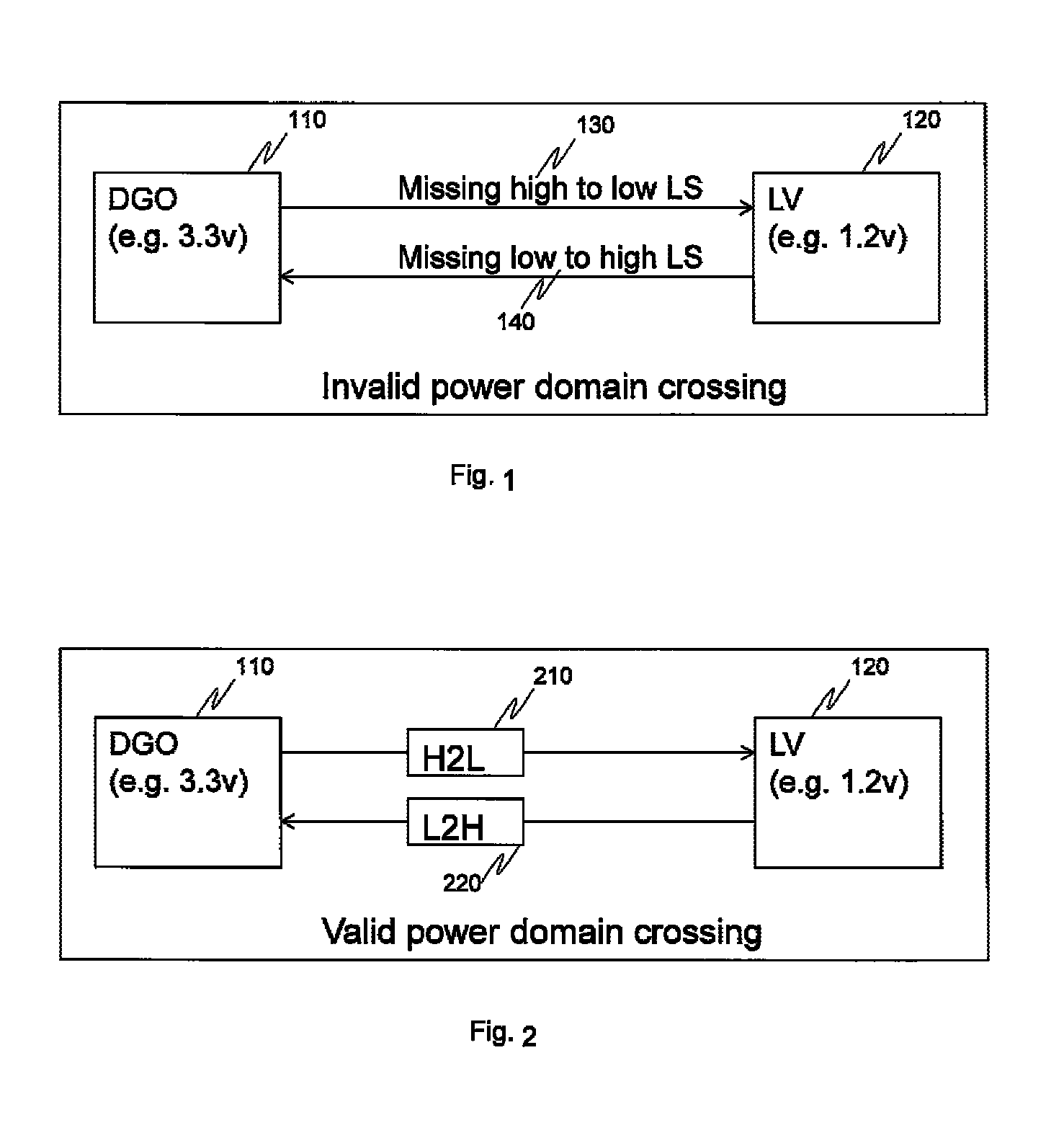
a multi-voltage domain, circuit design technology, applied in the direction of software simulation/interpretation/emulation, instruments, program control, etc., can solve problems such as invalid power domain crossing

Active Publication Date: 2013-12-03
NXP USA INC
View PDF17 Cites 12 Cited by
  • Summary
  • Abstract
  • Description
  • Claims
  • Application Information

AI Technical Summary

Problems solved by technology

If a level shifter is missing between two voltage ...

Method used


Image

  • Multi-voltage domain circuit design verification method
  • Multi-voltage domain circuit design verification method
  • Multi-voltage domain circuit design verification method

Examples


Embodiment Construction

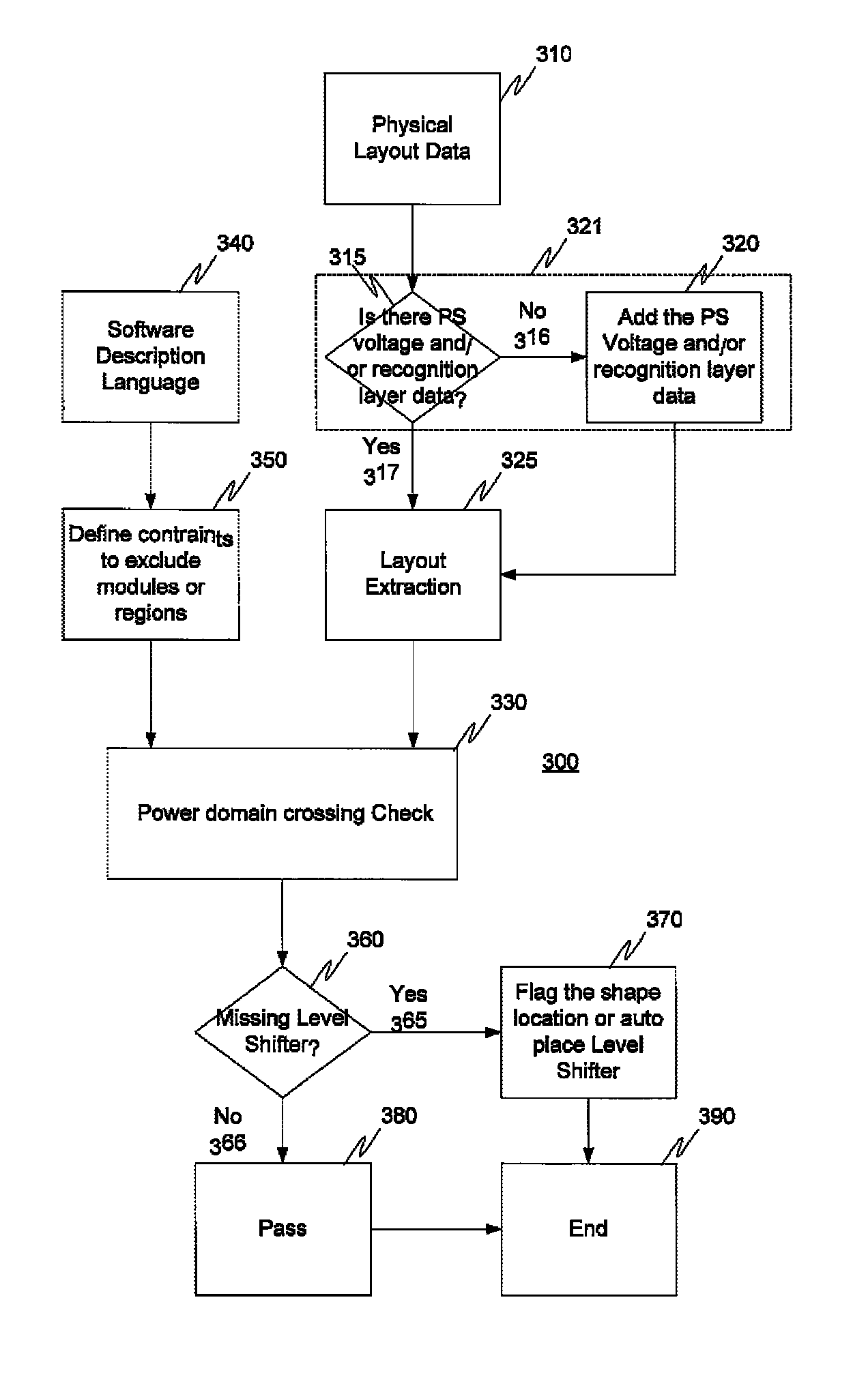
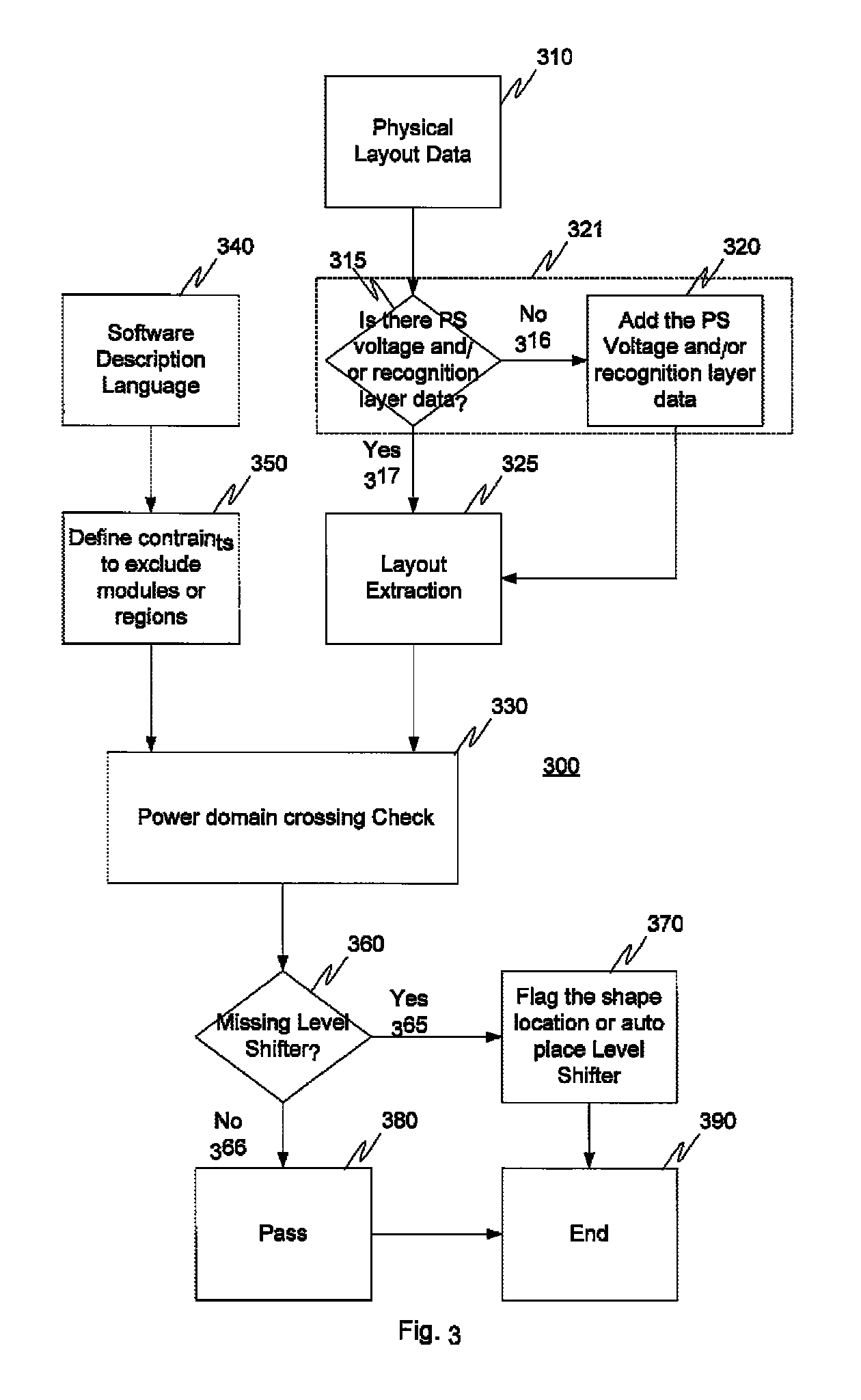
[0021]The present invention provides a method of identifying missing level shifters in a multi-voltage domain integrated circuit design. The present invention also provides an integrated circuit EDA system, or plug-in thereto, adapted to carry out the described method. These and other aspects of the invention will be apparent from and elucidated with reference to the embodiments described hereinafter.

[0022]The illustrated embodiments of the present invention may for the most part be implemented using electronic components and circuits known to those skilled in the art. Therefore, details will not be explained in any greater extent than that considered necessary as illustrated above, for the understanding and appreciation of the underlying concepts of the present invention and in order not to obfuscate or distract from the teachings of the present invention.

[0023]Main-stream EDA CAD tools for use in designing ICs often require the IC designer to define a complicated power specificati...


PUM


Abstract

A level shifter physical verification system identifies missing level shifters in a multi-voltage domain integrated circuit design. The system analyzes a physical layout design data file for design to identify domains and signals that cross domains, and connected nets of devices within the IC design having one or more missing level shifters.

Description

BACKGROUND OF THE INVENTION[0001]The present invention relates to the field of Integrated Circuit (IC) design using Electronic Design Automation (EDA) tools, and in particular, to a method and system for verifying level shifters in a multi-voltage IC design.[0002]IC design is now carried out using special Computer Aided Design (CAD) tools, sometimes known as EDA tools. These tools assist an IC designer to produce complex integrated circuitry, such as System on Chip (SoC) ICs, by not only assisting in the conversion of logical design parameters (from varying degrees of abstraction) into physical layout data for use in producing the semiconductor production masks, and the like, but also to aid in the testing of designs for correct operation and suitability for the chosen manufacturing process(es).[0003]Many IC designs today make use of multiple (different) voltage domains, where each domain may be supplied by a power supply voltage optimised for its task or structure. IC designers may...

Claims


Application Information

Patent Timeline
IPC IPC(8): G06F9/455G06F17/50
CPCG06F17/5081G06F2217/78G06F30/398G06F2119/06
Inventor DU, HUABIN
Owner NXP USA INC
Why Eureka
Try Eureka