Red phosphorescent compound and organic electroluminescent device using the same

a technology of red phosphorescent compound and organic electroluminescent device, which is applied in the direction of discharge tube luminescnet screen, other domestic articles, natural mineral layered products, etc., can solve the problems of reducing the spectral the difficulty of achieving high luminescence efficiency of the organic el device, etc., to achieve the desired chromaticity coordinate characteristics, high luminescence efficiency, and long luminescence lifetim

Active Publication Date: 2014-01-07
LG DISPLAY CO LTD
View PDF5 Cites 0 Cited by
  • Summary
  • Abstract
  • Description
  • Claims
  • Application Information

AI Technical Summary

Benefits of technology

[0014]An object of the present invention is to provide a red phosphorescent compound that exhibits desirable chromaticity coordinate characteristics (CIE color purity X>0.65), high luminescence efficiency, and long luminescence lifetime.

Problems solved by technology

As shown in FIG. 1, as the color purity of an organic EL device using a red phosphorescent material becomes higher (i.e. as the x-values on CIE chromaticity coordinates increase), the spectral luminous efficacy of the organic EL device decreases, making it difficult to achieve high luminescence efficiency of the organic EL device.

Method used


Image

  • Red phosphorescent compound and organic electroluminescent device using the same
  • Red phosphorescent compound and organic electroluminescent device using the same
  • Red phosphorescent compound and organic electroluminescent device using the same

Examples


example 1

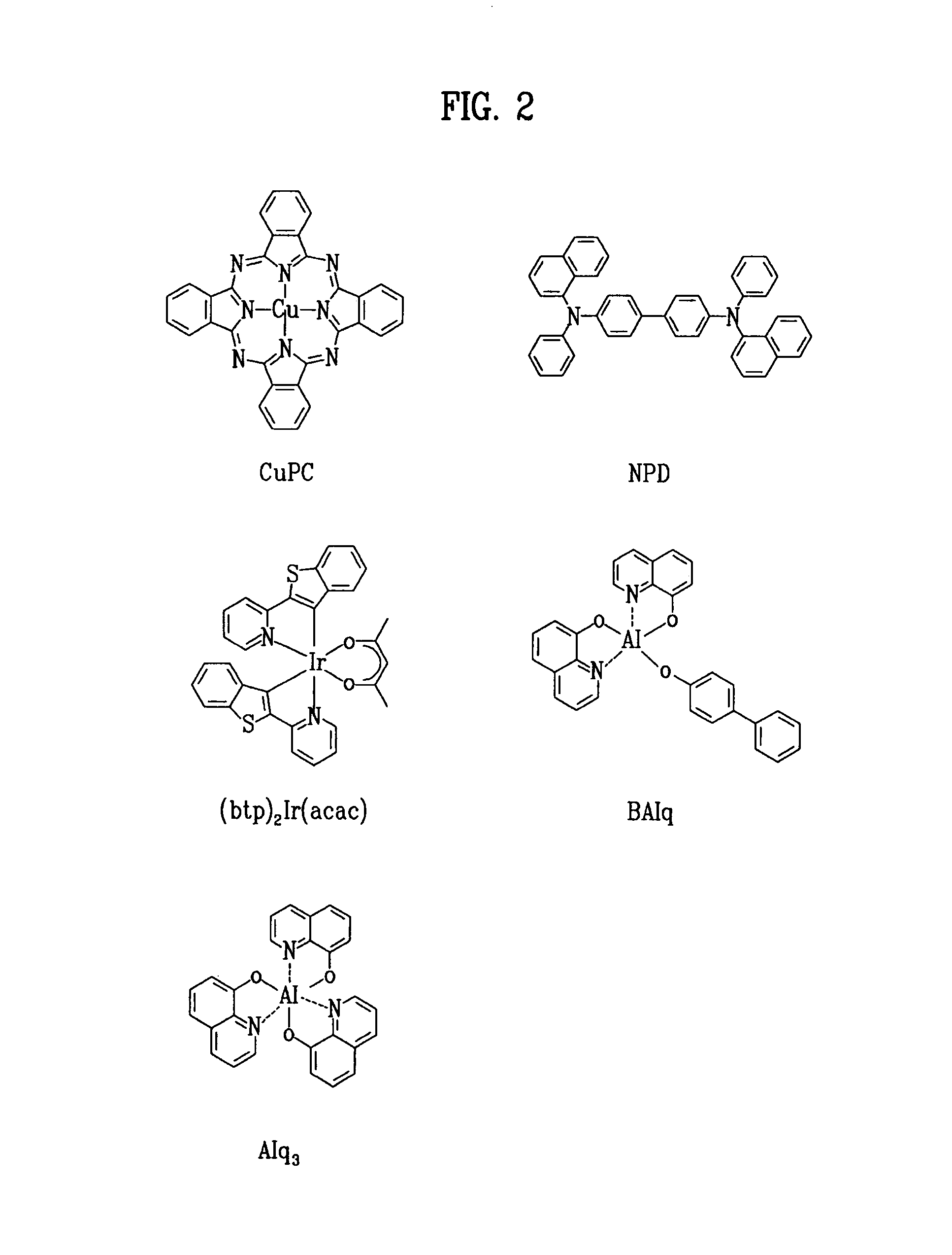
[0059]An ITO-coated glass substrate was patterned to have a light-emitting area of 3 mm×3 mm, followed by cleaning. After the patterned substrate was disposed in a vacuum chamber, the standard pressure of the chamber was adjusted to 1×10⁻⁶ torr. CuPc (200 Å), NPD (400 Å), BAlq+A-1 (7%) (200 Å), Alq3 (300 Å), LiF (5 Å) and Al (1,000 Å) were sequentially deposited on the ITO glass substrate to fabricate an organic EL device.

[0060]The luminance of the organic EL device thus fabricated was 1,326 cd / m2 at an electric current of 0.9 mA and a voltage of 6.1 V. At this time, the CIE chromaticity coordinates were x=0.601 and y=0.327. The lifetime (defined as the time taken before the luminance of the organic EL device decreases to half its initial value) of the organic EL device was 3,700 hours at 2,000 cd / m2.

example 2

[0061]An ITO-coated glass substrate was patterned to have a light-emitting area of 3 mm×3 mm, followed by cleaning. After the patterned substrate was disposed in a vacuum chamber, the standard pressure of the chamber was adjusted to 1×10⁻⁶ torr. CuPc (200 Å), NPD (400 Å), BAlq+A-2 (7%) (200 Å), Alq3 (300 Å), LiF (5 Å) and Al (1,000 Å) were sequentially deposited on the ITO glass substrate to fabricate an organic EL device.

[0062]The luminance of the organic EL device thus fabricated was 1,420 cd / m2 at an electric current of 0.9 mA and a voltage of 5.7 V. At this time, the CIE chromaticity coordinates were x=0.592 and y=0.330. The lifetime (defined as the time taken before the luminance of the organic EL device decreases to half its initial value) of the organic EL device was 4,200 hours at 2,000 cd / m2.

example 3

[0063]An ITO-coated glass substrate was patterned to have a light-emitting area of 3 mm×3 mm, followed by cleaning. After the patterned substrate was disposed in a vacuum chamber, the standard pressure of the chamber was adjusted to 1×10⁻⁶ torr. CuPc (200 Å), NPD (400 Å), BAlq+A-4 (7%) (200 Å), Alq3 (300 Å), LiF (5 Å) and Al (1,000 Å) were sequentially deposited on the ITO glass substrate to fabricate an organic EL device.

[0064]The luminance of the organic EL device was 1,320 cd / m2 at an electric current of 0.9 mA and a voltage of 5.8 V. At this time, the CIE chromaticity coordinates were x=0.621 and y=0.336. The lifetime (defined as the time taken before the luminance of the organic EL device decreases to half its initial value) of the organic EL device was 4,000 hours at 2,000 cd / m2.


PUM

PropertyMeasurementUnit
thicknessaaaaaaaaaa
thicknessaaaaaaaaaa
electric currentaaaaaaaaaa

Abstract

A red phosphorescent compound of Formula I:whereinisand R1, R2, R3, R4 and R5 are as defined in the specification.

Description

[0001]This application claims the benefit of Korean Patent Application No. 10-2006-0026630 filed on Mar. 23, 2006, which is hereby incorporated by reference as if fully set forth herein.BACKGROUND OF THE INVENTION[0002]1. Field of the Invention[0003]The present invention relates to a red light-emitting phosphorescent compound (hereinafter, referred to simply to as a ‘red phosphorescent compound’) and an organic electroluminescent (EL) device using the same. More particularly, the present invention relates to a red phosphorescent compound and an organic electroluminescent device realizing an improvement in color purity by using the red phosphorescent compound as a dopant of a light-emitting layer.[0004]2. Discussion of the Related Art[0005]Since electroluminescent devices are self-luminous display devices, they have the advantages of a wide viewing angle, a large contrast ratio, and a high response speed. Electroluminescent devices are divided into inorganic electroluminescent device...

Claims


Application Information

Patent Timeline
Patent Type & Authority Patents(United States)
IPC IPC(8): H01L51/54C09K11/06
CPCC09K2211/1029H01L51/0081C09K2211/1092C09K2211/185H01L51/5016H01L51/0085C09K11/06H05B33/14H10K85/324H10K85/342H10K50/11H10K2101/10C09K11/87Y10S428/917
Inventor KIM, JUNG KEUNSEO, JEONG DAELEE, KYUNG HOONPARK, CHUN GUNJEONG, HYUN CHEOLBIN, JONG KWANPIEH, SUNG HOON
Owner LG DISPLAY CO LTD
Why Eureka
Try Eureka