
Integrated design environment for nanophotonics

a nano-photonics and design environment technology, applied in the field of integrated electronic and photonic design methodologies, can solve the problems of insufficient present design technologies, high error-prone and time-consuming, immature photonic design tools, and lack of flexibility of electronic design tools

Active Publication Date: 2014-01-07
GLOBALFOUNDRIES U S INC
View PDF8 Cites 12 Cited by
  • Summary
  • Abstract
  • Description
  • Claims
  • Application Information

AI Technical Summary

Problems solved by technology

While electronic design is well established, nanophotonic integrated circuits are an emerging domain and present design technologies are inadequate.
Such methodologies, where two separate designs are merged, are highly error-prone and time-consuming.
Furthermore, photonic design tools are immature and lack the flexibility of electronic design tools.

Method used


Image

  • Integrated design environment for nanophotonics
  • Integrated design environment for nanophotonics
  • Integrated design environment for nanophotonics

Examples


Embodiment Construction

[0020]The present principles provide a unified design environment for electronic and photonic computer-aided design (CAD). Whereas previous attempts at integrated products were after-the-fact combinations of discrete electronic and photonic units, the present principles provide for the creation of integrated electronic / photonic circuits formed on a single substrate, thereby providing significant cost and performance benefits.

[0021]By integrating the design processes, the design environment can perform rule checking across both domains simultaneously, eliminating the tedious iterative reconciliation of two separate designs. In a typical design process, whether electronic of photonic, special layers and shapes are placed in a geometric space allocated to mask production that is used in integrated circuit manufacturing. The parameters for the layers and the shapes, including, e.g., length and width, have special-purpose meanings. For example, an RX layer is reserved for active transist...


PUM


Abstract

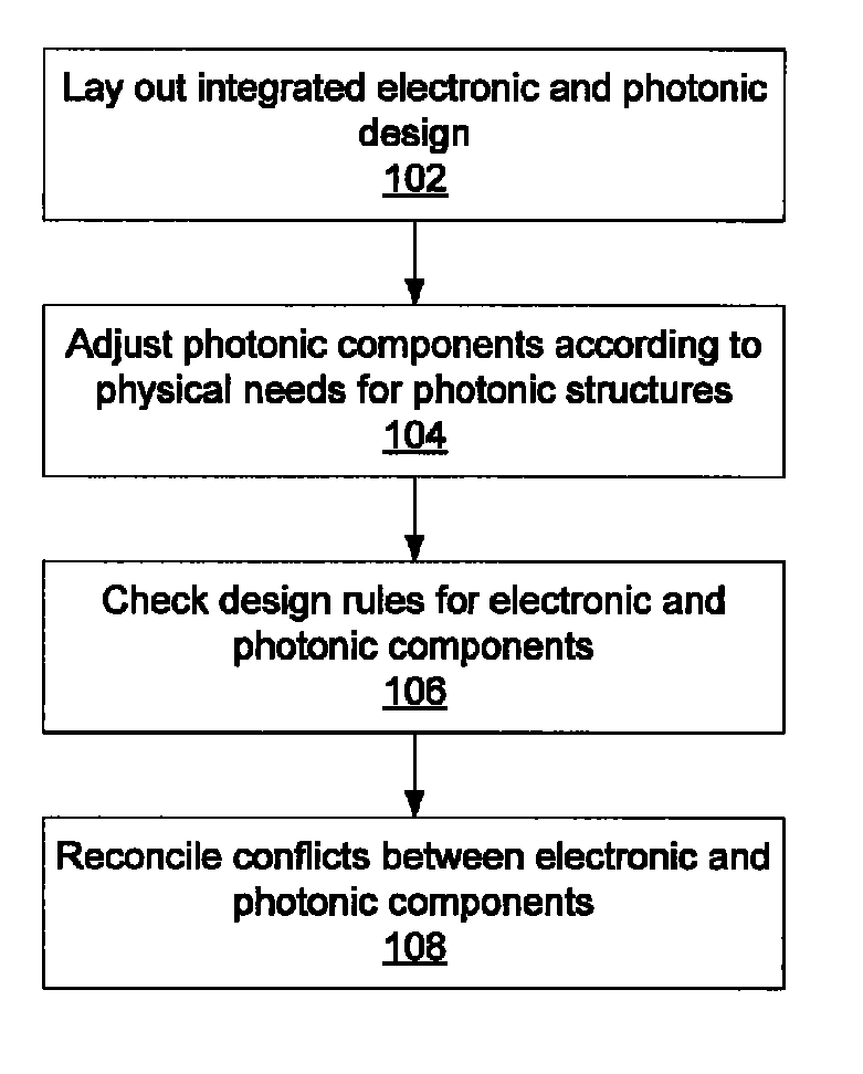
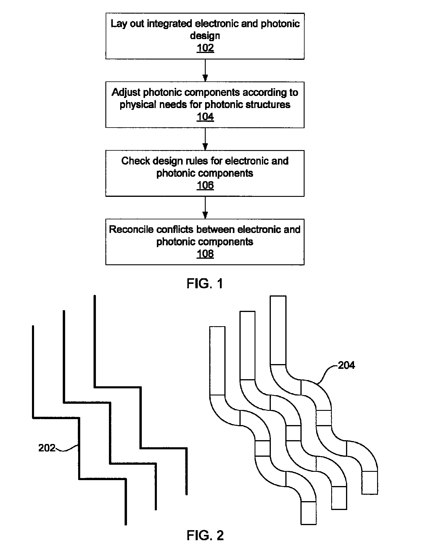
Methods for integrated electronic and photonic design include laying out electronic and photonic design components in a design environment; adjusting photonic components according to photonic design requirements using a processor; checking design rules for electronic and photonic components according to manufacturing requirements; and adjusting component positioning and size to reconcile conflicts between electronic and photonic components.

Description

BACKGROUND[0001]1. Technical Field[0002]The present invention relates to integrated electronic and photonic design methodologies and, more particularly, to design environments that incorporate both electronic and photonic elements.[0003]2. Description of the Related Art[0004]Designers of electronic devices and components frequently employ design tools to aid them. Such computer-aided design (CAD) makes use of automated rule checking and stock component types to allow a designer to rapidly create full circuit designs that conform to the requirements of the fabrication technology to be used.[0005]While electronic design is well established, nanophotonic integrated circuits are an emerging domain and present design technologies are inadequate. At present, integrated electronic / photonic devices undergo two wholly separate design processes, one in the electronic domain and one in the photonic domain, and designers must iterate back and forth to resolve conflicts and malfunctions. Such me...

Claims


Application Information

Patent Timeline
Patent Type & Authority Patents(United States)
IPC IPC(8): G06F17/50
CPCG06F17/50G06F17/5081G06F30/398G06F2119/18Y02P90/02
Inventor ACAR, EMRAHBEAKES, MICHAEL P.GREEN, WILLIAM M.PROESEL, JONATHAN E.RYLYAKOV, ALEXANDER V.VLASOV, YURII A.
Owner GLOBALFOUNDRIES U S INC
Learn More