Fabricating photonics devices fully integrated into a CMOS manufacturing process

a technology of photonics devices and manufacturing processes, applied in the field of integrated circuit processing of photonics devices, can solve the problems of germanium to form non-ohmic contacts, complicated integration of germanium into a conventional cmos process, etc., and achieve the effect of low resistan

Active Publication Date: 2012-05-24
GLOBALFOUNDRIES US INC
View PDF4 Cites 111 Cited by
  • Summary
  • Abstract
  • Description
  • Claims
  • Application Information

AI Technical Summary

Benefits of technology

[0006]According to a third aspect of the invention, there is provided a method of incorporating a photonics device into a CMOS manufacturing process flow including: providing a semiconductor substrate; processing a first portion of the semiconductor substrate according to a CMOS manufacturing process flow; processing a second portion of the semiconductor substrate according to a process flow for a photonics device which includes: patterning a semiconductor material layer in the semiconductor substrate to form first trenches between first pillars of semiconductor material; filling the first trenches with an insulator material; low dose implanting at least one of the first pillars to form a pn or p-i-n junction; and high dose implanting at least one of the first pillars to form a low resistance contact; and processing a third portion of the semiconductor substrate according to a process flow for a photonics device which includes: patterning a semiconductor material layer in the semiconductor substrate to form first trenches between first pillars of semiconductor material; tilling the first trenches with an insulator material; depositing a dielectric material over the second portion; opening a window in the dielectric material to expose an underlying first pillar of semiconductor material; depositing a layer of germanium over the first and second portions; depositing a first insulating layer over the germanium layer; patterning the germanium layer and first insulating layer over the first portion and removing the germanium layer and first insulating layer from the first portion; depositing a second insulating layer over the germanium layer and first insulating layer so as to encapsulate the germanium layer and first insulating layer.

Problems solved by technology

The integration of germanium into a conventional CMOS process is complicated by the additional thermal budget required by germanium growth, the maximum temperature germanium can withstand, cross-contamination issues, germanium doping issues, germanium passivation issues, and the tendency of germanium to form non-ohmic contacts when mated with those metallic materials conventionally used for vertical contacts.

Method used


Image

  • Fabricating photonics devices fully integrated into a CMOS manufacturing process
  • Fabricating photonics devices fully integrated into a CMOS manufacturing process
  • Fabricating photonics devices fully integrated into a CMOS manufacturing process

Examples


Embodiment Construction

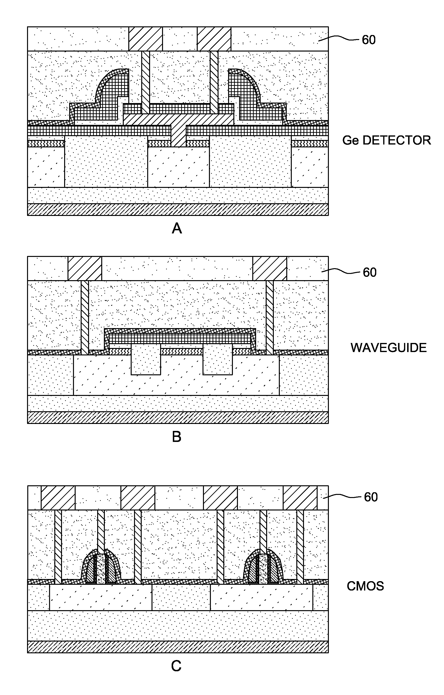
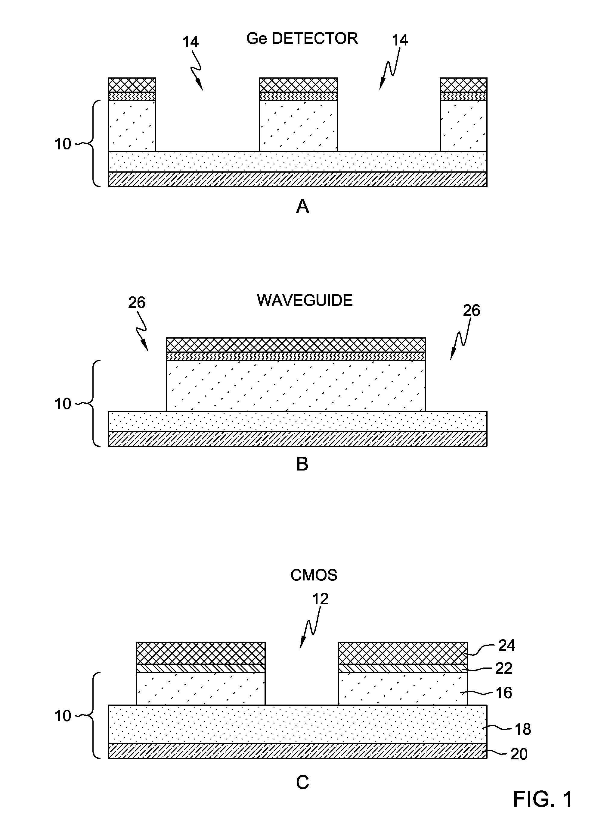
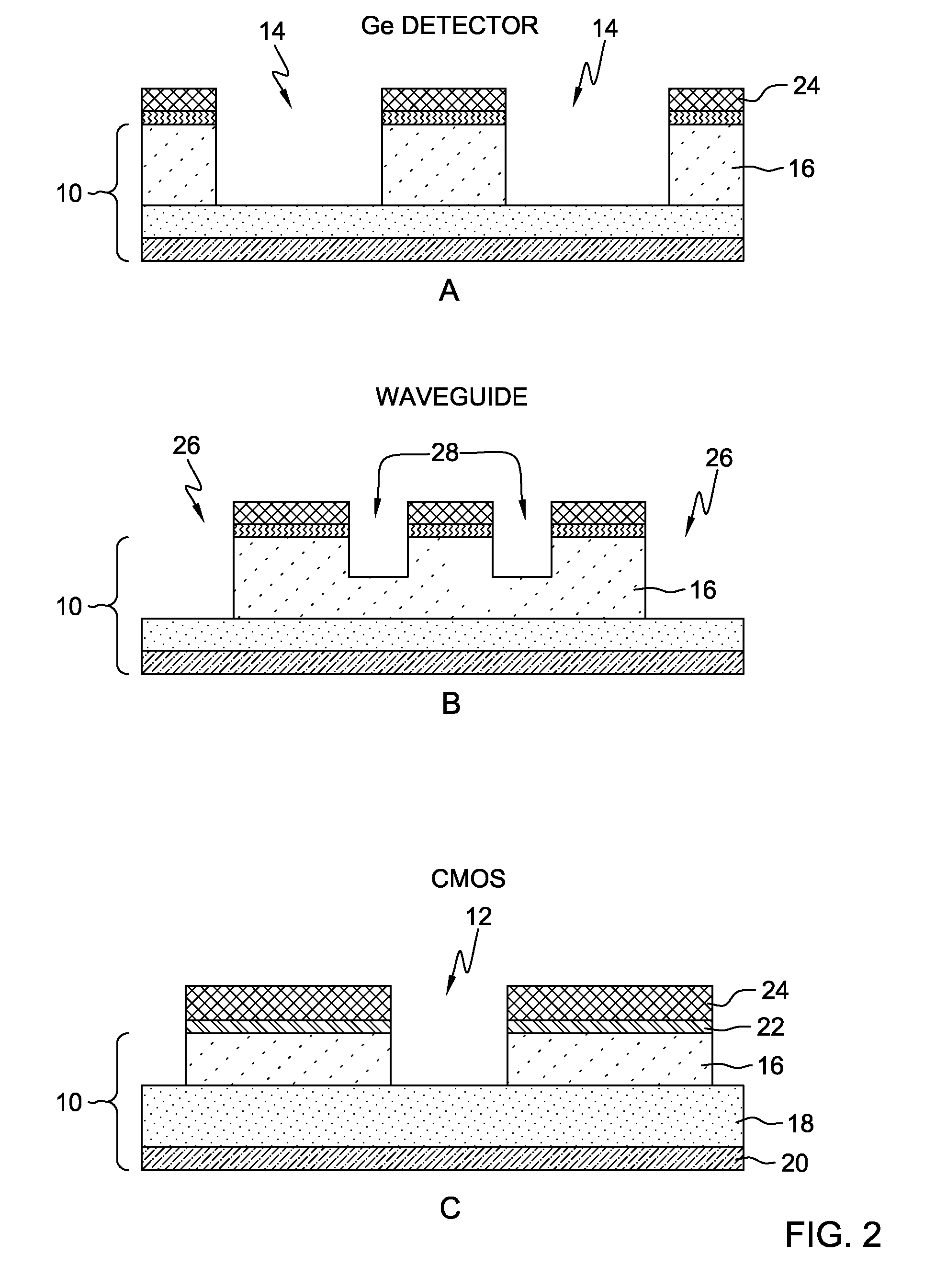
[0031]The present invention will be described with reference to exemplary embodiments. For this reason, numerous modifications can be made to these embodiments and the results will still come within the scope of the invention. No limitations with respect to the specific embodiments described herein are intended or should be inferred.

[0032]Particularly with respect to processing steps, it is emphasized that the descriptions provided herein are not intended to encompass all of the processing steps which may be required to successfully form a functional device in an integrated circuit. Rather, certain processing steps which are conventionally used in forming integrated circuit devices, such as, for example, wet cleaning and annealing steps which are not germane to the exemplary embodiments, are purposefully not described herein for economy of description. However one skilled in the art will readily recognize those processing steps omitted from this generalized description. Moreover, de...


PUM


Abstract

Disclosed are process enhancements to fully integrate the processing of a photonics device into a CMOS manufacturing process flow. A CMOS wafer may be divided into different portions. One of the portions is for the CMOS devices and one or more other portions are for the photonics devices. The photonics devices include a ridged waveguide and a germanium photodetector. The germanium photodetector may utilize a seeded crystallization from melt process so there is more flexibility in the processing of the germanium photodetector.

Description

BACKGROUND[0001]The exemplary embodiments relate generally to the processing of integrated circuits and, more particularly, relate to the processing of photonics devices integrated into the processing of integrated circuits.[0002]Optical interconnects can offer significant advantages over electrical circuitry in the field of advanced microelectronics. One possible implementation of an optical interconnect system is based on silicon-on-insulator (SOI) technology, in which optical waveguides are formed on the same thin silicon layer as other complimentary-metal-oxide-semiconductor (CMOS) circuit elements (e.g., field effect transistors (FETs), capacitors, resistors, etc.). Light sources produce optical signals (e.g., light pulses) that propagate in these optical waveguides. Photodetectors convert the optical signals into electrical signals.[0003]The integration of germanium into a conventional CMOS process is complicated by the additional thermal budget required by germanium growth, t...

Claims


Application Information

Patent Timeline
Patent Type & Authority Applications(United States)
IPC IPC(8): H01L21/782H01L21/762
CPCH01L21/26513H01L21/76283G02B6/136H01L21/8238H01L31/103H01L31/105H01L31/02327H01L21/2658
Inventor ASSEFA, SOLOMONGREEN, WILLIAM M.J.VLASOV, YURII A.YANG, MIN
Owner GLOBALFOUNDRIES US INC
Why Eureka
Try Eureka