Methods for nanoscale structures from optical lithography and subsequent lateral growth

a nanoscale structure and optical lithography technology, applied in the field of nanoscale lateral epitaxial growth methods and structures, can solve the problems of adverse effects on the electronic or optical properties of devices manufactured, gan dislocation or dislocation defects, and nitride semiconductor materials, etc., to reduce the effect of reducing the density of dislocation or d

Inactive Publication Date: 2007-02-08
NORTH CAROLINA STATE UNIV
View PDF3 Cites 115 Cited by
  • Summary
  • Abstract
  • Description
  • Claims
  • Application Information

AI Technical Summary

Benefits of technology

[0012] Periodic arrays with nanoscale features can therefore be formed in a substrate using a nanoscale lithography technique, such as edge definition lithography. Mesas or posts formed thereby can have a pitch of approximately 5-100 nm, and more particularly approximately 30-50 nm. The posts can be laterally overgrown to result in structures featuring sub-micron or nanoscale dimensions. The spacing between the laterally overgrown portions can be a nanoscale opening, for example with a spacing distance between adjacently grown lateral growth fronts which can be approximately 1-50 nm, and more particularly can be from approximately 3-5 nm, a spacing of nanoscale dimension appropriate for interconnection or integration of molecular electronic device elements. Using this technology, large-scale integration of nanoscale devices can be achieved using lithographic equipment that is orders of magnitude less expensive that that used for competing advanced lithographic techniques, such as electron beam lithography. The nanoscale patterning, growth and fabrication of multi-terminal interconnect nodes disclosed therefore have particular use in association with molecular electronics for device element attachment as the formation of mesas or posts is of a dimension less than the average distance characteristic between dislocation defects for example in GaN (ρ=1010 / cm2d→0.1 μm). Alternatively, the lateral overgrowth may proceed to complete coalescence leaving no gap between adjacent lateral growth fronts.
[0013] As the lateral growth periodicity is less than the average spacing between defects, a general reduction in defect density may be expected over the III-Nitride surface fabricated in this manner. The nanoscale patterning of features and subsequent lateral overgrowth have use as a technique to achieve III-Nitride semiconductor materials of reduced dislocation or defect density. Layers fabricated in this method may be used in association with electronic or photonic devices benefiting from low defect densities such as LEDs, laser diodes, photo detectors or transistors.

Problems solved by technology

A major problem that has typically been associated with the fabrication of GaN-based microelectronic devices is the threading dislocations or dislocation defects that can be formed in GaN due to differences in lattice constants and differences in the coefficients of thermal expansion between GaN III-Nitride and its substrate (lattice mismatch).
The dislocations originate in the general area of the III-Nitride-substrate interface and can have adverse effects on the electronic or optical properties of devices fabricated on or containing III-Nitride semiconductor materials.
The layer can also contain structural defects such as point defects, misfit dislocations, and stacking faults.
While lateral growth has produced significant results in improved crystal quality, lateral growth has not been applied to fabricating three-dimensional active layers or interconnect layers in devices.

Method used


Image

  • Methods for nanoscale structures from optical lithography and subsequent lateral growth
  • Methods for nanoscale structures from optical lithography and subsequent lateral growth
  • Methods for nanoscale structures from optical lithography and subsequent lateral growth

Examples


Embodiment Construction

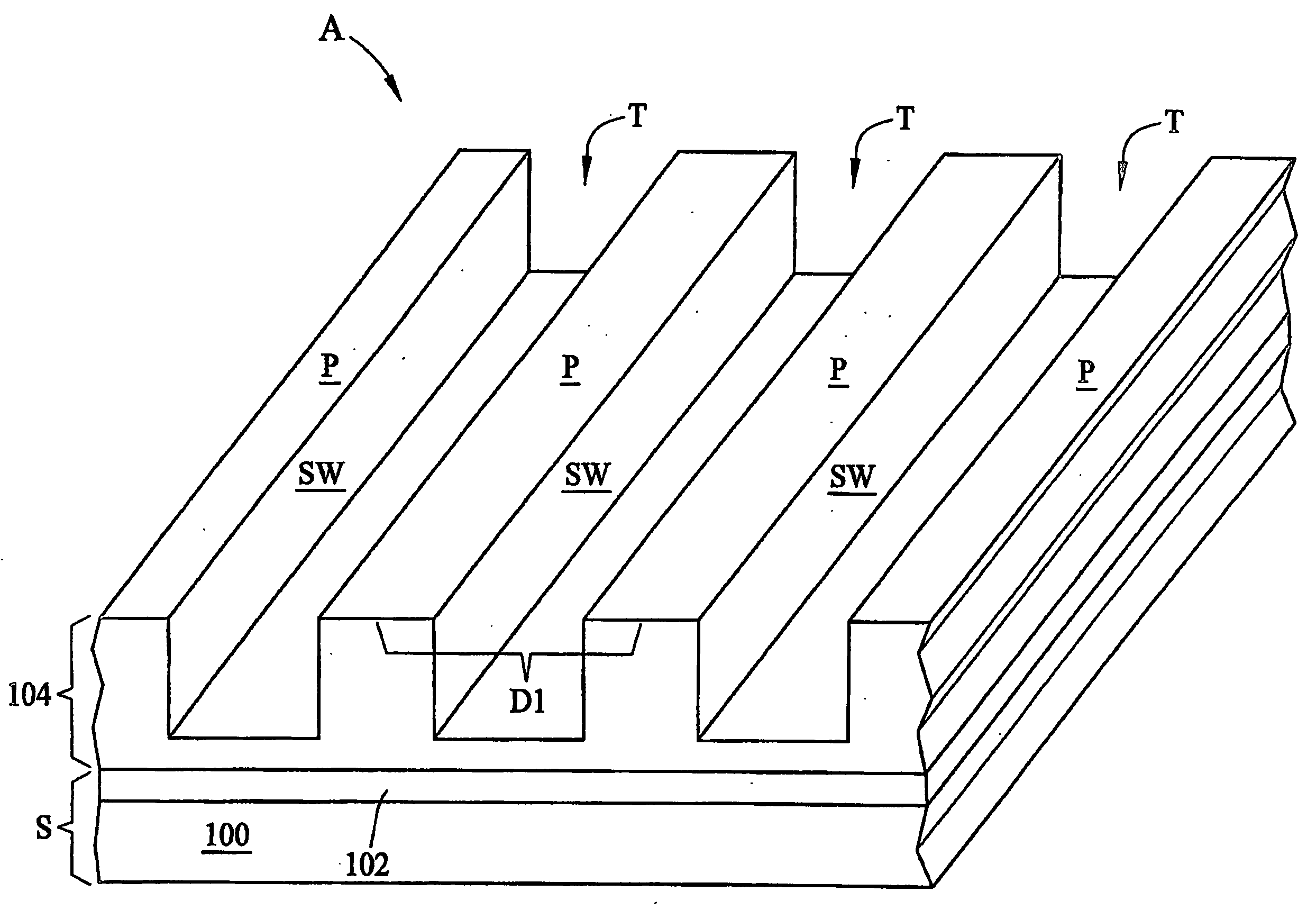
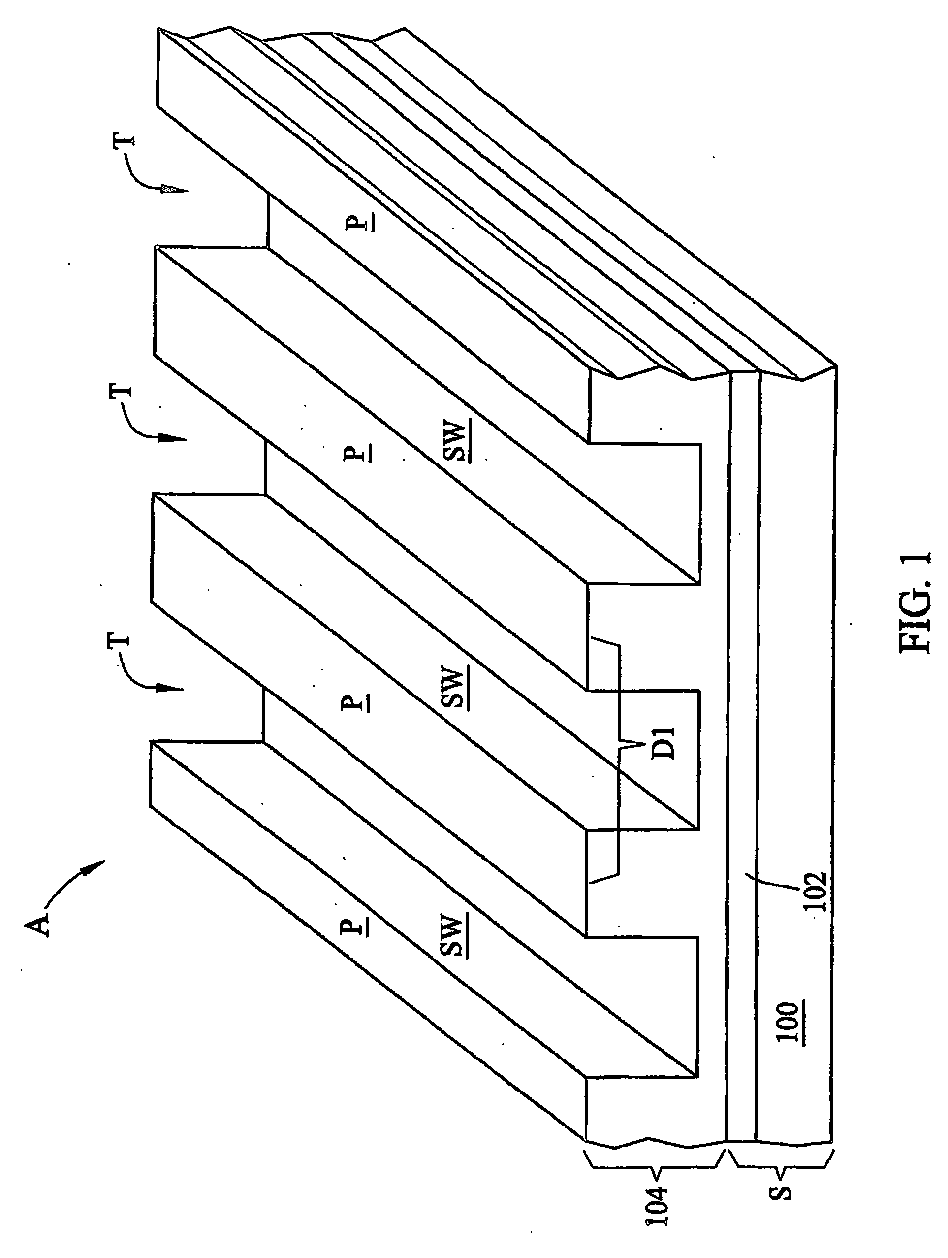
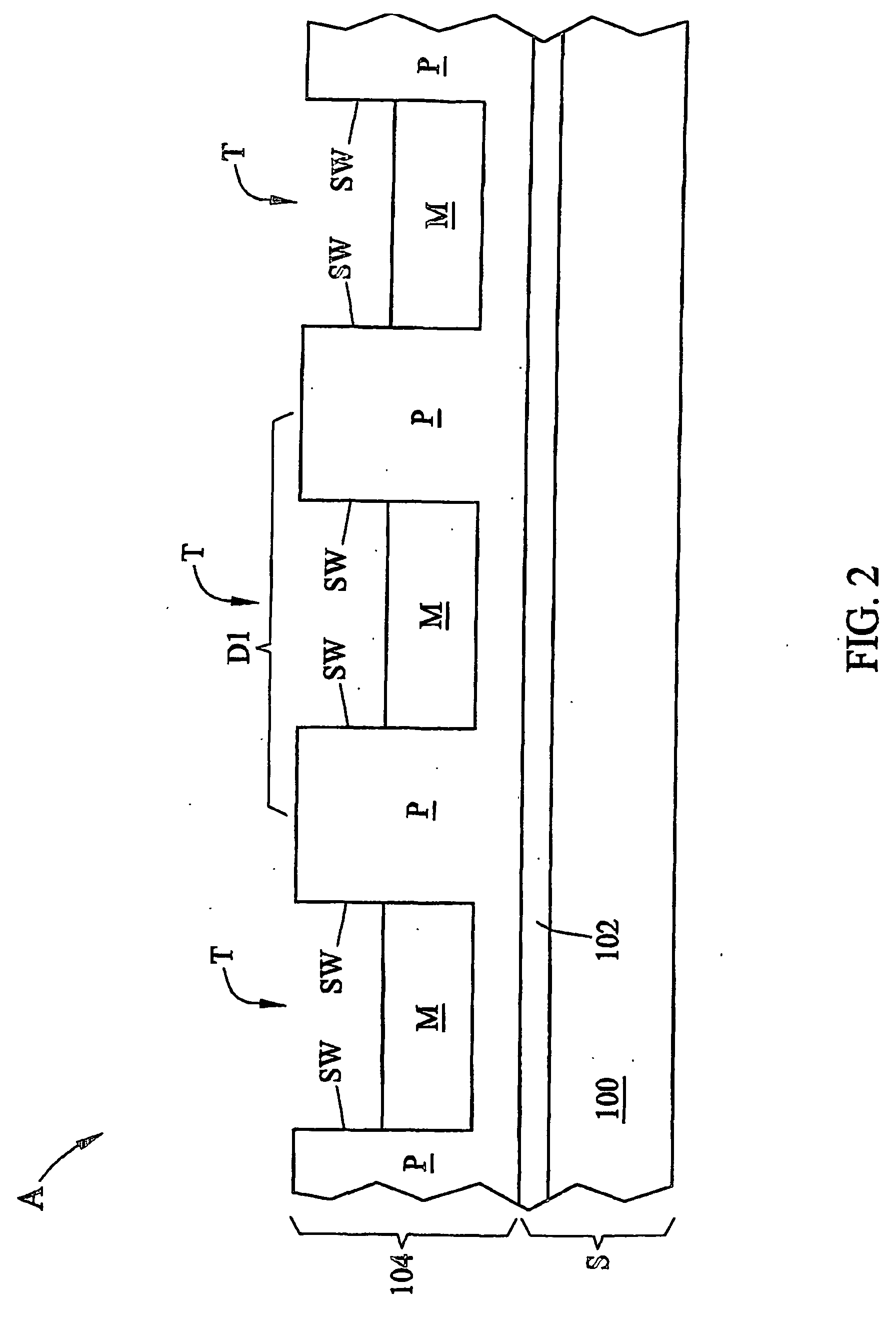
[0027] The present subject matter discloses methods, and structures formed thereby, for forming laterally grown structures with nanoscale dimensions from nanoscale arrays patterned from nanoscale lithography, such as for example and without limitation, edge defined lithography or another lithography method capable of achieving features of a nanoscale dimensional size. The structures and methods disclosed herein have applications with, for example and without limitation, electronic, photonic, molecular electronic, spintronic, microfluidic or nano-electromechanical (NEMS) technologies.

[0028] A wide bandgap semiconductor can be used such as Group III nitrides, particularly gallium nitride (GaN). As used herein and appreciated by those of skill in the art, GaN includes alloys of GaN such as aluminum nitride, indium nitride, aluminum gallium nitride, indium gallium nitride and aluminum indium gallium nitride. While the description herein often uses GaN as an example of a material suitab...


PUM

PropertyMeasurementUnit
widthaaaaaaaaaa
widthaaaaaaaaaa
spacing distanceaaaaaaaaaa

Abstract

Methods, and structures formed thereby, are disclosed for forming laterally grown structures with nanoscale dimensions from nanoscale arrays which can be patterned from nanoscale lithography. The structures and methods disclosed herein have applications with electronic, photonic, molecular electronic, spintronic, microfluidic or nano-mechanical (NEMS) technologies. The spacing between laterally grown structures can be a nanoscale measurement, for example with a spacing distance which can be approximately 1-50 nm, and more particularly can be from approximately 3-5 nm. This spacing is appropriate for integration of molecular electronic devices. The pitch between posts can be less than the average distance characteristic between dislocation defects for example in GaN (ρ=1010/cm2→d=0.1 μm) resulting an overall reduction in defect density. Large-scale integration of nanoscale devices can be achieved using lithographic equipment that is orders of magnitude less expensive that that used for advanced lithographic techniques, such as electron beam lithography.

Description

RELATED APPLICATIONS [0001] This application claims the benefit of U.S. Provisional Patent Applications Ser. Nos. 60 / 456,775 and 60 / 456,770, both filed Mar. 21, 2003, the disclosures of which are incorporated by reference in their entireties. This application relates to co-pending U.S. patent application entitled “METHODS AND SYSTEMS FOR SINGLE- OR MULTI-PERIOD EDGE DEFINITION LITHOGRAPHY”, commonly owned and filed on even date herewith, the disclosure of which is incorporated herein by reference in its entirety.TECHNICAL FIELD [0002] The present disclosure relates generally to nanoscale lateral epitaxial growth methods and structures. More particularly, the present disclosure relates to methods, and structures formed thereby, for forming laterally grown structures with nanoscale features from nanoscale arrays patterned from sub-micron lithography. BACKGROUND ART [0003] In making semiconductor and nanoscale devices, it is often desirable to make features of increasingly small size i...

Claims


Application Information

Patent Timeline
Patent Type & Authority Applications(United States)
IPC IPC(8): H01L23/58B81C1/00H01L21/285H01L21/331H01L21/335
CPCB81C1/00111B81C1/00619B82Y10/00B82Y30/00H01L21/0237H01L29/66462H01L21/0254H01L21/02639H01L21/0265H01L21/28587H01L29/66318H01L21/0243
Inventor JOHNSON, MARK ALAN LAMONTEBARLAGE, DOUGLAS WILLIAMMUTH, JOHN
Owner NORTH CAROLINA STATE UNIV
Why Eureka
Try Eureka