Solid-state imaging device, method of manufacturing solid-state imaging device, and electronic apparatus

a solid-state imaging and manufacturing method technology, applied in the direction of radio frequency controlled devices, transistors, television systems, etc., can solve the problems of overflow path, difficult to control the potential in a region on the lower side of (in a region separate) and become more difficult to control the variations in impurity concentration, etc., to achieve high image quality and high quality

Inactive Publication Date: 2014-01-14
SONY CORP
View PDF4 Cites 42 Cited by
  • Summary
  • Abstract
  • Description
  • Claims
  • Application Information

AI Technical Summary

Benefits of technology

[0010]However, in the CMOS image sensor of the structure described in Patent Document 1, the potential barrier of the overflow path between the photodiode and the electric-charge holding region may be easily varied by variations in the impurity concentration arising from scattering results of production. Particularly, it becomes more difficult to control variations in impurity concentration as the pixel size is reduced and the pixel structure becomes finer.
[0013]Where the predetermined signal charge cannot be stably accumulated in the photodiode, as above-mentioned, the quality of images picked up would be lowered. Thus, there is a need for suppressing the variations of potential in the region on the lower side of the overflow path in each pixel possessed by a solid-state imaging device, and thereby enhancing the quality of images picked up.
[0014]Thus, there is a desire to obtain images with enhanced image quality.
[0019]According to the above-described embodiments of the present invention, images with high image quality can be obtained and a solid-state imaging device capable of producing images with high quality can be manufactured.

Problems solved by technology

Particularly, it becomes more difficult to control variations in impurity concentration as the pixel size is reduced and the pixel structure becomes finer.
Specifically, in the structure of the overflow path described in Patent Document 1, the potential barrier of the overflow path is determined by a single impurity layer, and, at the time of realizing a predetermined potential barrier, it is difficult to control the potential in a region on the lower side of (in a region separate in the depth direction from) the overflow path.
Especially, in the case where the area of each unit pixel is reduced attendant on the reduction of chip size of the CMOS image sensor, the potential in the region on the lower side of the overflow path becomes more susceptible to influences of the photodiode and the electric-charge holding region, whereby the potential may vary more.
With the region on the lower side of the overflow path thus influenced by the photodiode and the electric-charge holding region, a punch-through phenomenon due to a short channel effect becomes more liable to occur, and it becomes difficult to accumulate a predetermined signal charge stably in the photodiode.

Method used


Image

  • Solid-state imaging device, method of manufacturing solid-state imaging device, and electronic apparatus
  • Solid-state imaging device, method of manufacturing solid-state imaging device, and electronic apparatus
  • Solid-state imaging device, method of manufacturing solid-state imaging device, and electronic apparatus

Examples


first embodiment

[First Embodiment]

[0077]Now, the configuration of unit pixels 120A in a first embodiment will be described below referring to FIGS. 3A to 4C. In FIGS. 3A to 4C and in the following drawings, the same components as those in the unit pixel of FIG. 2 above will be denoted by the same reference symbols as used above, and detailed descriptions of them will be omitted.

[0078]FIG. 3A is a plan view showing the configuration of the unit pixel 120A, and FIG. 3B is a sectional view of the unit pixel 120A along line A-A′ in the plan view of FIG. 3A.

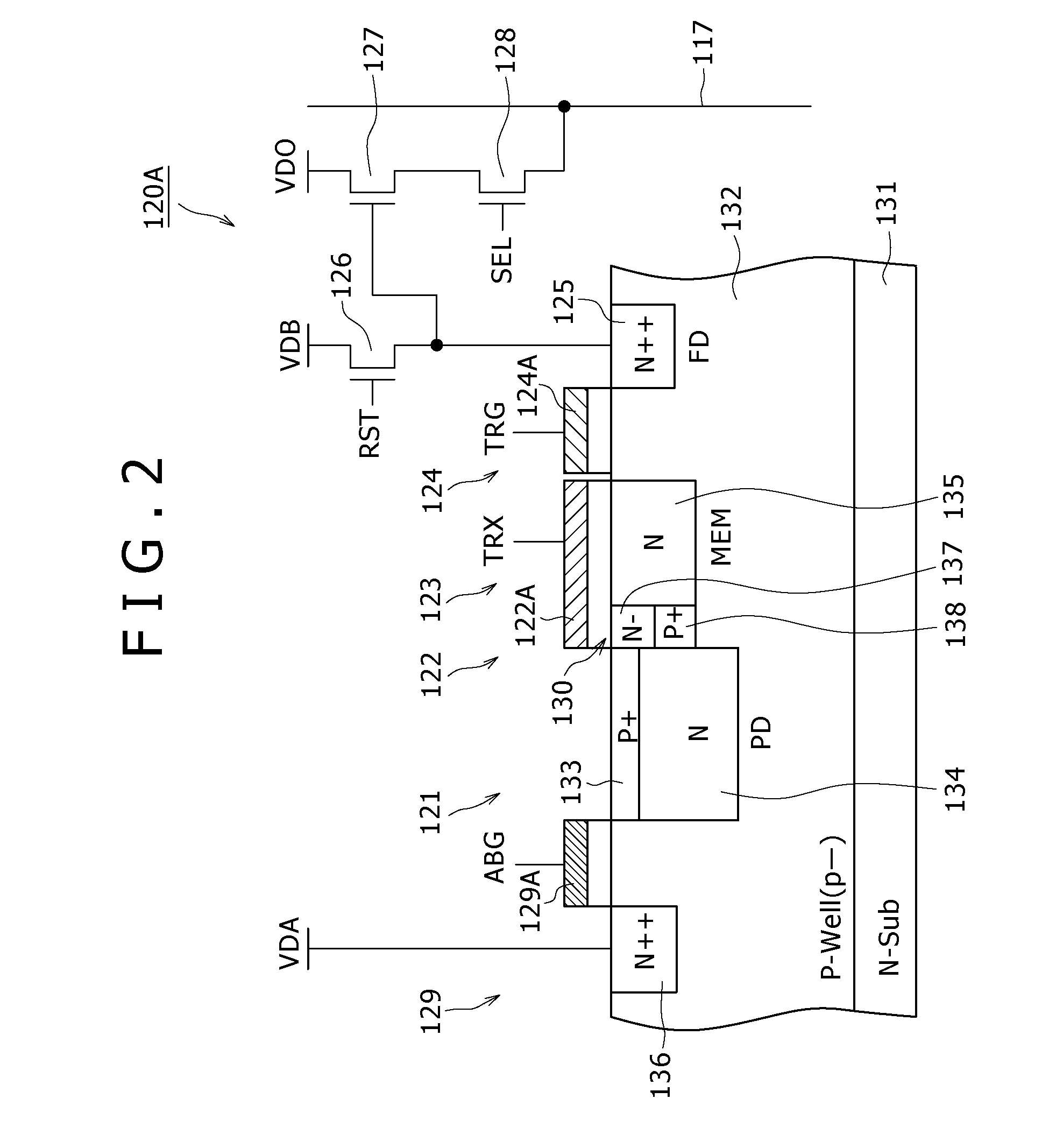
[0079]As shown in FIGS. 3A and 3B, a photodiode 121, a memory part 123, and a floating diffusion region 125 are disposed in the unit pixel 120A. The photodiode 121 and the memory part 123 are formed to have such an impurity concentration that a depletion state is obtained upon discharging of electric charge. The floating diffusion region 125 is formed to have an impurity concentration such as to permit electrical connection therewith of a wiring cont...

second embodiment

[Second Embodiment]

[0100]FIG. 6 shows a sectional view of a unit pixel 120B according to a second embodiment.

[0101]As shown in FIG. 6, in the unit pixel 120B, an impurity diffusion region 138B formed on the lower side of an impurity diffusion region 137 which becomes an overflow path 130 is so formed as to extend to the lower side (the substrate depth side) of a part or a whole part of a buried channel 135 constituting a memory part 123. In other words, the impurity diffusion region 138 is formed to be L-shaped in section shown in FIG. 6.

[0102]With the impurity diffusion region 138B thus extending to the lower side of the buried channel 135, a potential barrier similar to that between the N-type buried layer 134 and the buried channel 135 is formed also on the lower side of the memory part 123. As a result, the punch-through phenomenon which would take place between the N-type buried layer 134 and the buried channel 135 in the unit pixel 120B can be prevented from occurring. In addi...

third embodiment

[Third Embodiment]

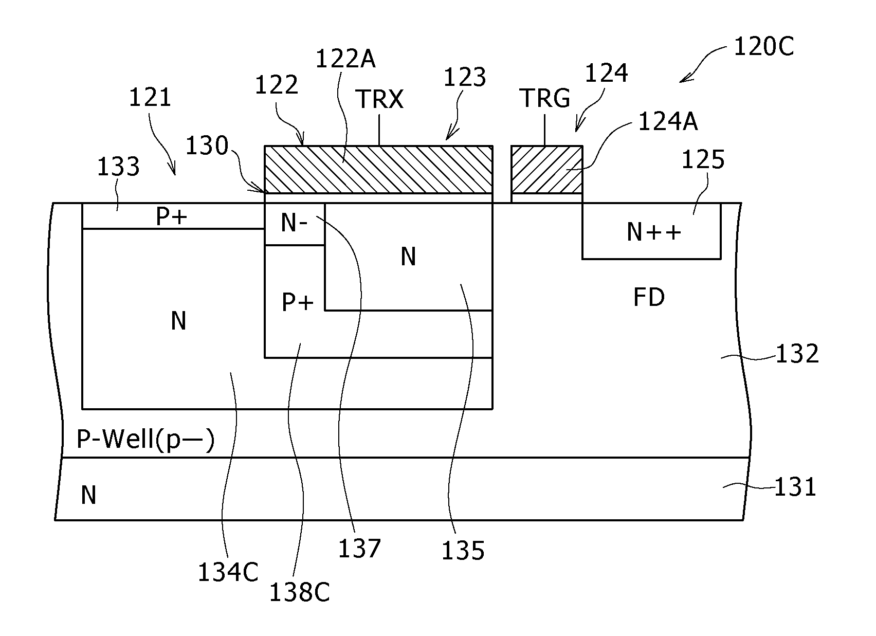
[0111]FIG. 9 is a sectional view of a unit pixel 120C according to a third embodiment.

[0112]As shown in FIG. 9, in the unit pixel 120C, an impurity diffusion region 138C formed on the lower side of an impurity diffusion region 137 which becomes an overflow path 130 is extending to the lower side of a buried channel 135 constituting a memory part 123, like in the impurity diffusion region 138B of FIG. 6. Further, in the unit pixel 120C, an N-type buried layer 134C constituting a photodiode 121 is formed so as to extend to the lower side of the impurity diffusion region 138C. In other words, the impurity diffusion region 138C and the N-type buried layer 134C are formed to be L-shaped in section shown in FIG. 9.

[0113]With the N-type buried layer 134C thus extending to the lower side of the buried channel 135, formation of the overflow path 130 can be stabilized. Further, the electric charge generated through photoelectric conversion by light incident on a P-type well ...


PUM


Abstract

Disclosed herein is a solid-state imaging device including: a semiconductor region of a second conductivity type which is formed on a face side of a semiconductor substrate; a photoelectric conversion element which has an impurity region of a first conductivity type and which is operable to generate electric charge according to the amount of incident light and to accumulate the electric charge in the inside thereof; an electric-charge holding region which has an impurity region of the first conductivity type and in which the electric charge generated through photoelectric conversion by the photoelectric conversion element is held until read out; an intermediate transfer path through which only the electric charge generated by the photoelectric conversion element during an exposure period and being in excess of a predetermined electric charge amount is transferred into the electric-charge holding region; and an impurity layer.

Description

BACKGROUND OF THE INVENTION[0001]1. Field of the Invention[0002]The present invention relates to a solid-state imaging device, a method of manufacturing a solid-state imaging device, and an electronic apparatus. In particular, the invention relates to a solid-state imaging device, a method of manufacturing the solid-state imaging device, and an electronic apparatus using the solid-state imaging device by which images with high quality can be obtained.[0003]2. Description of the Related Art[0004]Solid-state imaging devices have been incorporated in various electronic apparatuses, for example, imaging apparatuses such as digital still cameras, video cameras, etc. and mobile terminal apparatuses having an imaging function, for a variety of uses. The solid-state imaging devices include APS (active pixel sensor) having amplifying elements on a pixel basis, and CMOS (complementary MOS) image sensors in which signal charges accumulated in photodiodes provided as photoelectric conversion el...

Claims


Application Information

Patent Timeline
Patent Type & Authority Patents(United States)
IPC IPC(8): H01L27/146
CPCH01L27/14607H01L27/14656H01L27/1461H04N5/37452H01L27/14616H04N25/771
Inventor OHRI, HIROYUKIMACHIDA, TAKASHIKAWAMURA, TAKAHIROSOGOH, YASUNORI
Owner SONY CORP
Why Eureka
Try Eureka