Memory transistor with multiple charge storing layers and a high work function gate electrode

a memory transistor and gate electrode technology, applied in the field of memory transistors, can solve the problems of limited useful transistor lifetime, incompatible current process for forming performance of memory transistors with those used for fabricating logic transistors, and only moderate improvement of eol 106/b>

Active Publication Date: 2014-01-21
LONGITUDE FLASH MEMORY SOLUTIONS LTD
View PDF74 Cites 25 Cited by
  • Summary
  • Abstract
  • Description
  • Claims
  • Application Information

AI Technical Summary

Benefits of technology

[0009]The present invention provides a solution to these and other problems, and offers further advantages over conventional memory cells or devices and methods of fabricating the same.

Problems solved by technology

One problem with conventional memory transistors and methods of forming the same is that the charge trapping layer typically has poor or decreasing data retention over time, limiting the useful transistor lifetime.
Moreover, the slope of Vt in retention mode is still appreciably steep and the leakage path is not sufficiently minimized to significantly improve data retention, thus EOL 106 is only moderately improved.
Another problem is that increasingly semiconductor memories combine logic transistors, such as MOSFET's, with memory transistors in integrated circuits (ICs) fabricated on a common substrate for embedded memory or System-On-Chip (SOC) applications.
Many of the current processes for forming performance of memory transistors are incompatible with those used for fabricating logic transistors.

Method used


Image

  • Memory transistor with multiple charge storing layers and a high work function gate electrode
  • Memory transistor with multiple charge storing layers and a high work function gate electrode
  • Memory transistor with multiple charge storing layers and a high work function gate electrode

Examples


Embodiment Construction

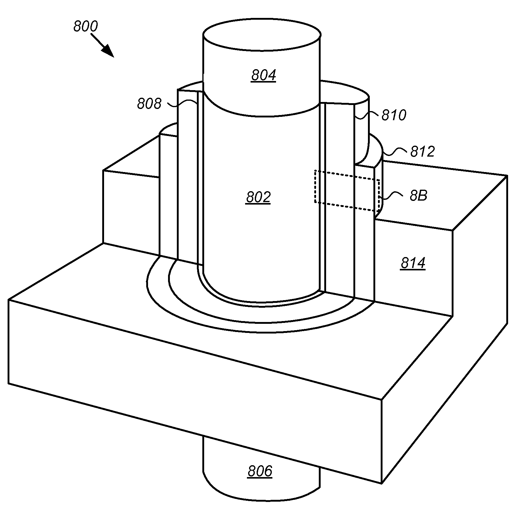
[0025]The present invention is directed generally to non-volatile memory transistor including a multi-layer charge storage layer and high work function gate electrode to increase data retention and / or to improve programming time and efficiency. The structure and method are particularly useful for embedded memory or System-On-Chip (SOC) applications in which a semiconductor device includes both a logic transistor and non-volatile memory transistor comprising high work function gate electrodes formed on a common substrate.

[0026]In the following description, for purposes of explanation, numerous specific details are set forth in order to provide a thorough understanding of the present invention. It will be evident, however, to one skilled in the art that the present invention may be practiced without these specific details. In other instances, well-known structures, and techniques are not shown in detail or are shown in block diagram form in order to avoid unnecessarily obscuring an un...


PUM


Abstract

A semiconductor devices including non-volatile memories and methods of fabricating the same to improve performance thereof are provided. Generally, the device includes a memory transistor comprising a polysilicon channel region electrically connecting a source region and a drain region formed in a substrate, an oxide-nitride-nitride-oxide (ONNO) stack disposed above the channel region, and a high work function gate electrode formed over a surface of the ONNO stack. In one embodiment the ONNO stack includes a multi-layer charge-trapping region including an oxygen-rich first nitride layer and an oxygen-lean second nitride layer disposed above the first nitride layer. Other embodiments are also disclosed.

Description

CROSS-REFERENCE TO RELATED APPLICATIONS[0001]This application is a continuation-in-part of co-pending U.S. application Ser. No. 13 / 288,919, filed Nov. 3, 2011, which is a divisional of U.S. application Ser. No. 12 / 152,518, filed on May 13, 2008, now U.S. Pat. No. 8,063,434, issued on Nov. 22, 2011, which claims the benefit of priority under 35 U.S.C. 119(e) to U.S. Provisional Patent Application Ser. No. 60 / 940,160, filed May 25, 2007, all of which application are hereby incorporated by reference in their entirety.TECHNICAL FIELD[0002]The present invention relates generally to semiconductor devices, and more particularly to integrated circuits including non-volatile semiconductor memories and methods of fabricating the same.BACKGROUND[0003]Non-volatile semiconductor memories are devices that can be electrically erased and reprogrammed. One type of non-volatile memory that is widely used for general storage and transfer of data in and between computers and other electronic devices is...

Claims


Application Information

Patent Timeline
Patent Type & Authority Patents(United States)
IPC IPC(8): H01L29/792
CPCH01L21/28282H01L29/66833B82Y10/00G11C16/04H01L27/11563H01L29/4234H01L29/518H01L29/513H01L29/4916H01L29/511H01L29/792H01L27/11526G11C16/0466H01L29/7926H01L29/40117H10B41/40H10B43/00H10B43/30H10B43/40H10B43/50H01L21/0214H01L21/02532H01L21/02595H01L29/0676H01L29/66795H01L29/0649H01L29/42344H01L29/512
Inventor POLISHCHUK, IGORLEVY, SAGYRAMKUMAR, KRISHNASWAMY
Owner LONGITUDE FLASH MEMORY SOLUTIONS LTD
Why Eureka
Try Eureka