Packaging photon building blocks having only top side connections in a molded interconnect structure

a technology of photon building blocks and interconnection structures, applied in the field of packaging lightemitting diodes, can solve the problems of not being able to connect the pads to a power source, phosphor and silicone are expensive, and the array products are not conventionally manufactured, so as to achieve the effect of efficient and less costly

Active Publication Date: 2014-02-18
BRIDGELUX INC
View PDF31 Cites 6 Cited by
  • Summary
  • Abstract
  • Description
  • Claims
  • Application Information

AI Technical Summary

Benefits of technology

[0011]Systems and methods for manufacturing and processing LED devices using standard semiconductor packaging technologies and equipment are disclosed. The systems and methods enable LED package sizes to be shrunk to sizes that are smaller than can be made using conventional LED packaging technologies. In addition, a more efficient and less costly interface interconnect between an LED die / array and the packaging is disclosed.
[0028]In one example, each microdot of HR material has a diameter of less than 100 microns and is typically 50-80 microns in diameter. The HR material has an adequately low viscosity (less than 1100 cP) such that it flows laterally to some degree once it reaches the substrate surface. Due to the lateral flow of the HR material, the HR material can be made (1) to flow under bridging wire bonds and to coat the substrate underneath the wire bonds, (2) to reach and to wet side edges of the LED dice, or (3) to reach and to wet the inside side edge of a phosphor retaining ring. In one example, the area of substrate between LED dice is not coated with HR material in order to reduce manufacturing time. Because the HR material is only deposited after die attach and after wire bonding, fiducial markers on the upper surface of the substrate (that would otherwise be covered and obscured by HR material were conventional screen printing used to deposit the HR material) are observable and usable during die attach and wire bonding. The depositing of the HR layer by jetting microdots of HR material results in a reduction in the amount of exposed substrate area that is not covered with HR material. Reducing the amount of exposed substrate area that is not covered with HR material serves to improve the light efficiency of the resulting LED assembly.

Problems solved by technology

Array products are not conventionally made using the discrete light emitters as building blocks.
But eliminating the through-hole vias by connecting the LED chips to pads on the top side of the carrier substrate creates the new problem of how to connect the pads to a power source because the carrier substrate is no longer electrically coupled to the printed circuit board below.
First, the phosphor and the silicone are expensive, and the lens material that is squeezed out of the cavities is wasted.
Second, the quality of the lenses formed with injection molding and casting molding is low because bubbles and nonuniformities remain in the finished product.
Fabricating an LED lens using these techniques is expensive because there are significant material losses and because non-standard semiconductor packaging technologies and equipment are used to package the lens.
However, the layer of silicone is not disposed laterally above a portion of the contact pad because the silicone has been removed by blasting abrasive particles in a stream of air at the layer of silicone.
Limits on mechanical tolerances can lead to physical differences between the LED assemblies being manufactured.

Method used


Image

  • Packaging photon building blocks having only top side connections in a molded interconnect structure
  • Packaging photon building blocks having only top side connections in a molded interconnect structure
  • Packaging photon building blocks having only top side connections in a molded interconnect structure

Examples


Embodiment Construction

[0110]Reference will now be made in detail to some embodiments of the invention, examples of which are illustrated in the accompanying drawings.

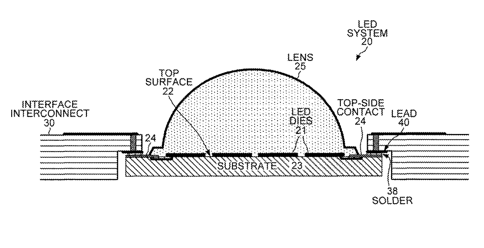
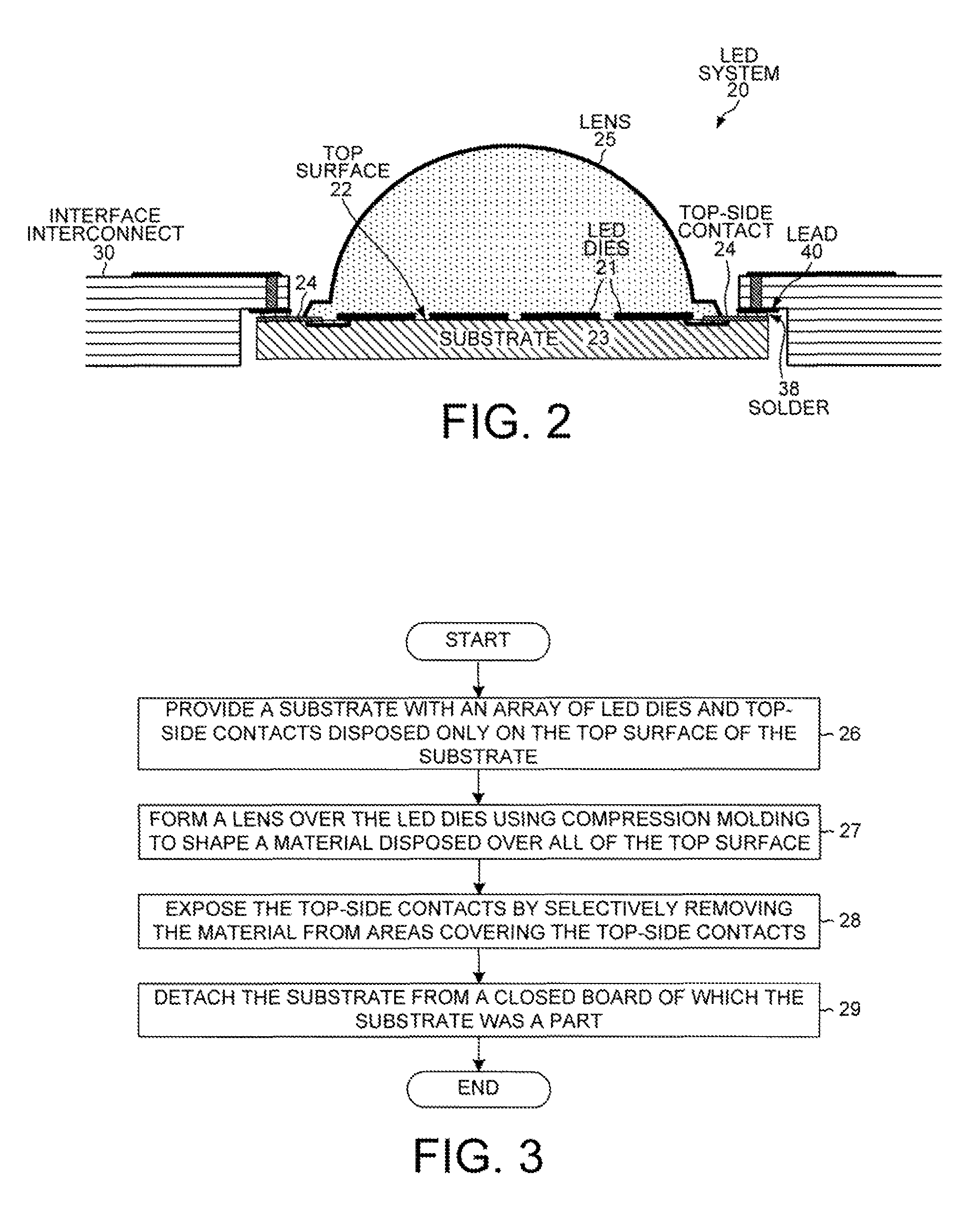
[0111]Systems and methods for manufacturing and processing LED devices using standard semiconductor packaging technologies and equipment are disclosed. The systems and methods enable LED package sizes to be shrunk to sizes that are smaller than can be made using conventional LED packaging technologies. In addition, a more efficient and less costly interface interconnect between an LED die / array and the packaging is disclosed.

[0112]In one embodiment, an LED is fabricated by providing a substrate with an array of LED dies and top-side contacts. One or more lenses are formed over the array of LED dies using compression molding such that one lens is formed over at least one of the LED dies. The top-side contacts are exposed by selectively removing material from areas covering the top-side contacts. Fabricating LED lens in this manner enables low...


PUM


Abstract

Standardized photon building blocks are packaged in molded interconnect structures to form a variety of LED array products. No electrical conductors pass between the top and bottom surfaces of the substrate upon which LED dies are mounted. Microdots of highly reflective material are jetted onto the top surface. Landing pads on the top surface of the substrate are attached to contact pads disposed on the underside of a lip of the interconnect structure. In a solder reflow process, the photon building blocks self-align within the interconnect structure. Conductors in the interconnect structure are electrically coupled to the LED dies in the photon building blocks through the contact pads and landing pads. Compression molding is used to form lenses over the LED dies and leaves a flash layer of silicone covering the landing pads. The flash layer laterally above the landing pads is removed by blasting particles at the flash layer.

Description

CROSS REFERENCE TO RELATED APPLICATION[0001]This application is a continuation-in-part of, and claims priority under 35 U.S.C. §120 from, the following three nonprovisional U.S. patent applications: patent application Ser. No. 12 / 987,148 entitled “Packaging Photon Building Blocks Having Only Top Side Connections in an Interconnect Structure,” filed on Jan. 9, 2011; patent application Ser. No. 13 / 284,835 entitled “Jetting a Highly Reflective Layer onto an LED Assembly,” filed on Oct. 28, 2011; and patent application Ser. No. 13 / 304,769 entitled “Micro-Bead Blasting Process for Removing a Silicone Flash Layer,” filed on Nov. 28, 2011. In addition, this application claims priority under 35 U.S.C. §119 from U.S. Provisional Patent Application Ser. No. 61 / 594,371 entitled “Packaging Photon Building Blocks Having Only Top Side Connections in a Molded Interconnect Structure,” filed on Feb. 2, 2012. The subject matter of each of the aforementioned patent documents is incorporated herein by ...

Claims


Application Information

Patent Timeline
Patent Type & Authority Patents(United States)
IPC IPC(8): H01L21/00
CPCH01L2224/45144H01L2224/48137H01L2224/48227H01L2933/0058H01L25/0753H01L2224/73265H01L33/54H01L33/62H01L33/60H01L2224/48091H01L2933/005H01L2924/07811H01L2224/49113H01L2924/00014H01L2924/00H01L33/486H01L33/58H01L33/642H01L2933/0066H01L2933/0075H01L33/505H01L33/64H01L2933/0041
Inventor WEST, R. SCOTTTONG, TAOKWON, MIKESOLOMENSKY, MICHAEL
Owner BRIDGELUX INC
Why Eureka
Try Eureka