Parasitic capacitance cancellation in capacitive measurement applications

a capacitance measurement and parasitic technology, applied in the direction of resistance/reactance/impedence, instruments, pulse techniques, etc., can solve problems such as degrading performance in these applications, and achieve the effect of negating the effect of the capacitance in the measurement system

Active Publication Date: 2014-02-25
AZOTEQ HLDG LTD
View PDF7 Cites 14 Cited by
  • Summary
  • Abstract
  • Description
  • Claims
  • Application Information

AI Technical Summary

Benefits of technology

[0008]The sensitivity of the process can be increased by reducing the effective value of CM. This means that not only can the parasitic capacitances be removed, but that CM can be adjusted to have a specific capacitance. This must be done without a physical change to the sensor structure (sense plate / antenna). One way to implement this is described hereinafter.
[0013]Firstly, the current mirror structure is well suited for scaling the current. Thus the reference current (IR) flowing from CPC can be mirrored (IR:IS). The notation 1:1 means the exact same current will flow in the secondary circuit; 1:0.5 (or 2:1) gives 50% of the current in the secondary; and 1:2 results in the current in the secondary circuit being doubled. This enables the designer to scale the capacitors, such as CPC, in order to optimise for performance, cost, signal to noise ratio or other design parameters.
[0014]Secondly, since the charge on CR continuously changes as CR is being charged to the trip level, it is not that simple to remove the correct charge in a constant manner. However, in this embodiment the CPC is charged to a fixed level or discharged from a fixed level to create the reference current. Because of the current mirror operation and characteristics the secondary circuit current (IS) flowing from CR is independent of the voltage level of CR. This means the charge added to CR due to the parasitic capacitance can be removed in a way that is constant in every charge / discharge cycle i.e. essentially in the same way that it is added. This provides for a linear operation in removing charge from the CR. This, coupled with the implementation described below for handling the charge transfers from CM in the same manner, allows a more linear system is achieved.
[0016]In a further embodiment the current mirror or other mirror element can have a ratio between the IR and IS currents. For example if the ratio is a step down ratio of a 1000 then it is possible to reduce the value of CR a 1000 times and still get the same number of transfers. This means a CR that may not be practical to embed in a normal CMOS IC (e.g. 20 nF) can be reduced to a value that can very reasonably be implemented on-chip (e.g. 20 pF). This results in significant savings in cost through reducing discrete components (cost and manufacturing) as well as reducing pin count, or coupling of noise.

Problems solved by technology

Inherent parasitic capacitances associated with sense plates, switches, connections and wiring degrade performance in these applications.

Method used


Image

  • Parasitic capacitance cancellation in capacitive measurement applications
  • Parasitic capacitance cancellation in capacitive measurement applications
  • Parasitic capacitance cancellation in capacitive measurement applications

Examples


Embodiment Construction

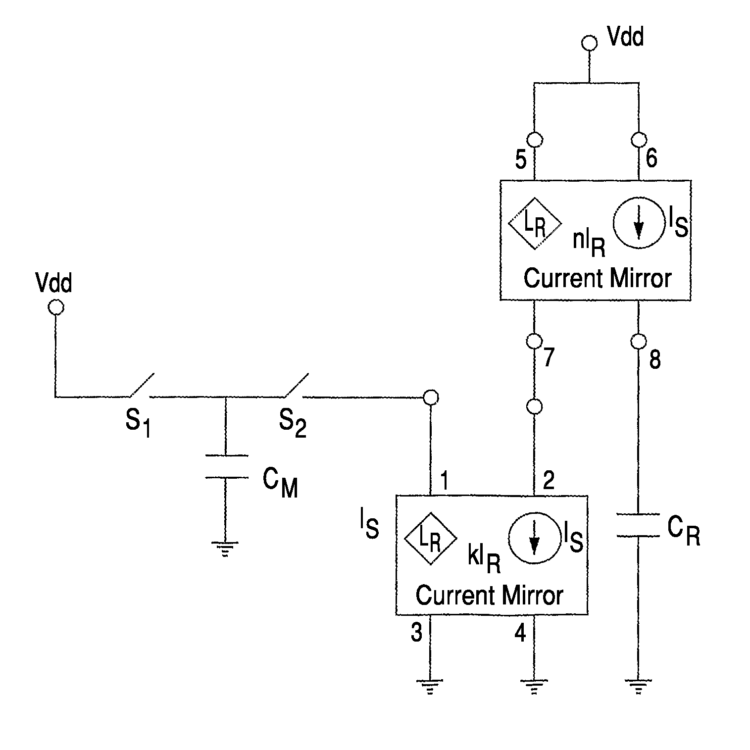
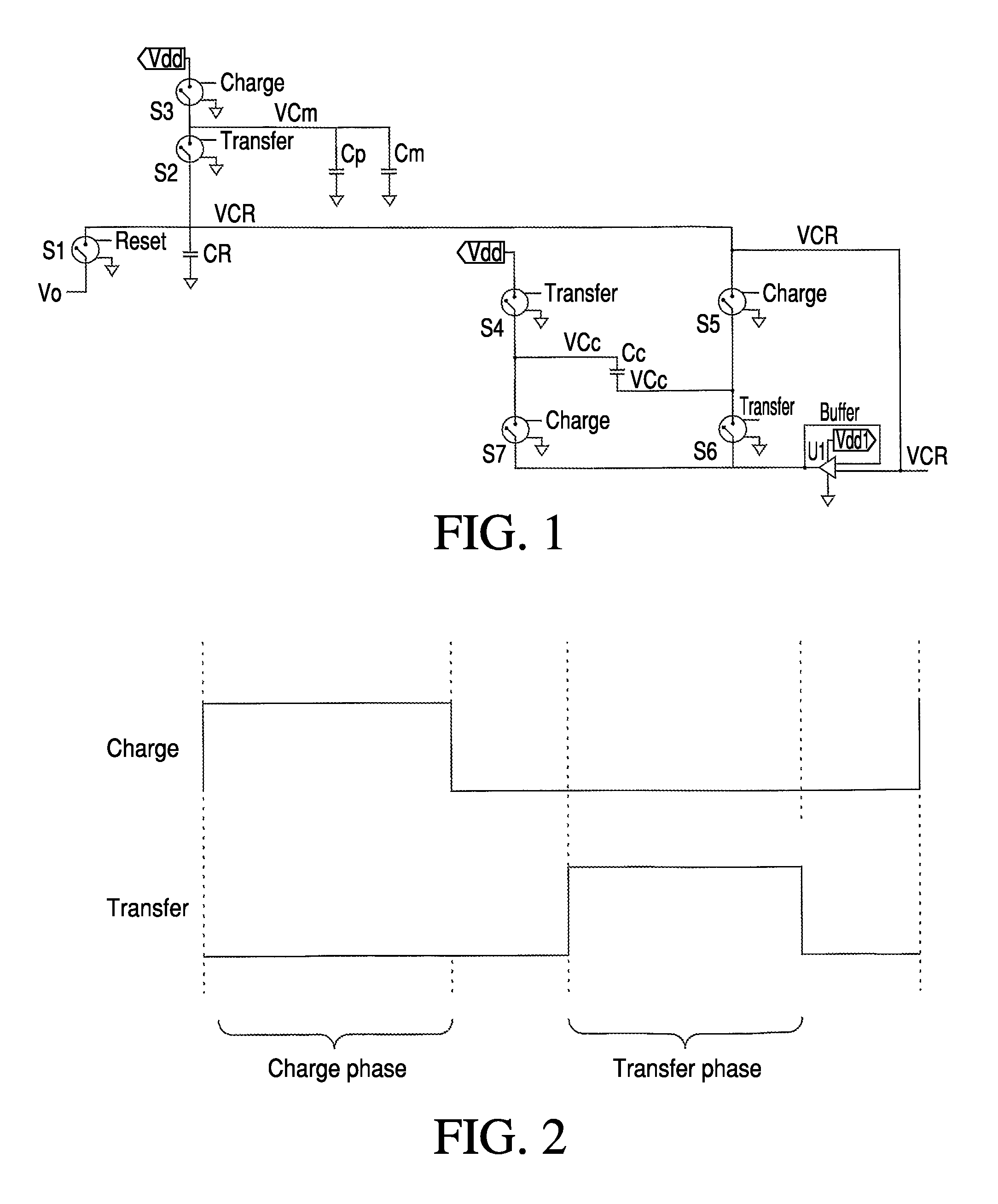
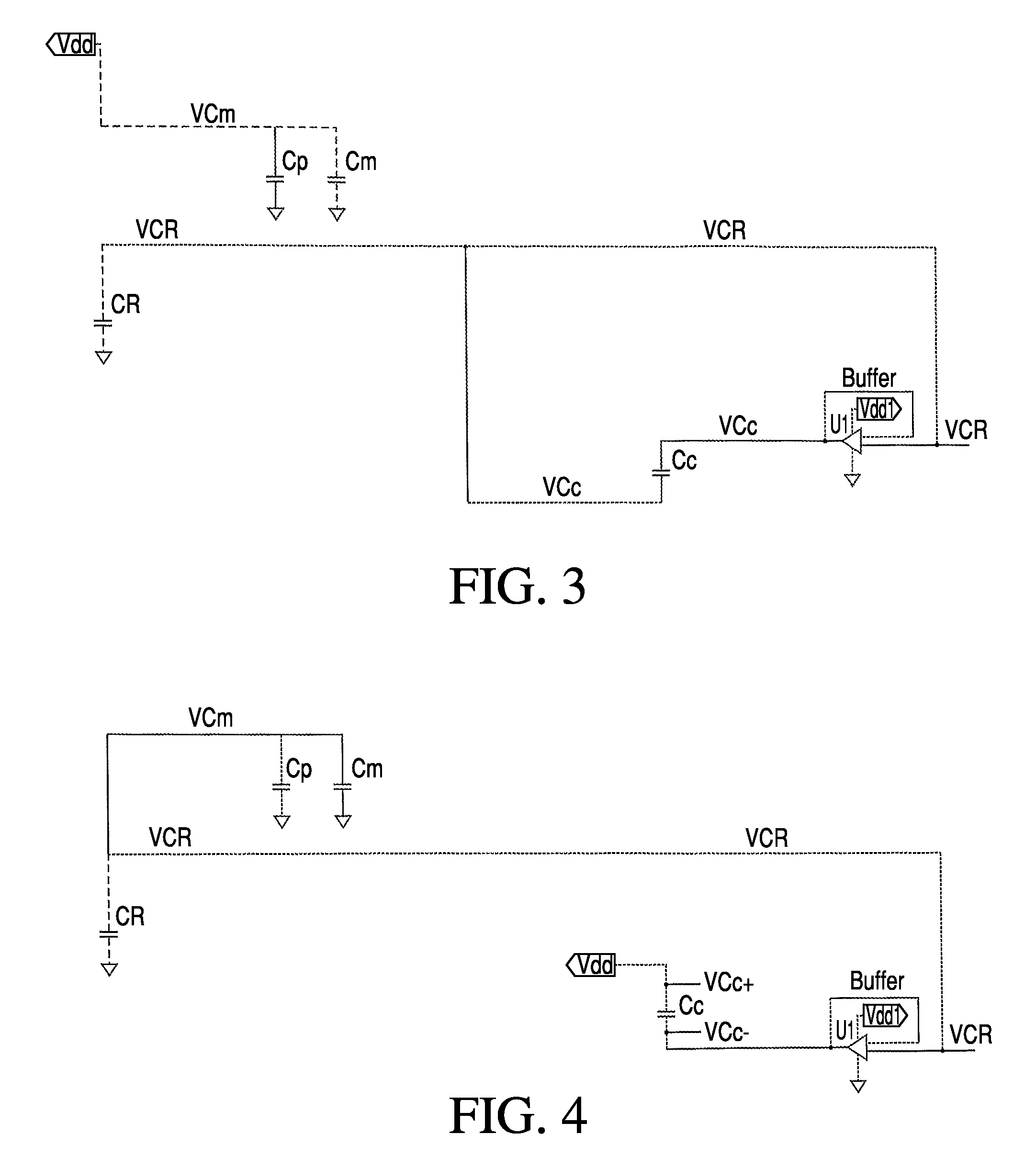
[0043]FIG. 1 shows a charge transfer circuit as well as a parasitic capacitance cancellation circuit.

[0044]Before a “measurement period” a reference capacitor (CR) is initialized to a known voltage Va (e.g. 0V) by closing a switch S1.

[0045]The Charge Transfer Cycle consists of at least 4 phases, viz the Charge Phase (UP), the Transfer Phase (PASS) and two Deadtime Phases (FIG. 2) which ensure that the Charge Phase and the Transfer Phase do not overlap. During the Charge Phase switches S3, S5 and S7 are closed and switches S2, S4 and S6 are open. A measured capacitor (CM) as well as the parasitic capacitance (CP) are charged to a reference voltage (Vdd).

[0046]During the Transfer Phase the switches S2, S4 and S6 are closed and the switches S3, S5 and S7 are open. Capacitors CM and CP are connected to the reference capacitor (CR) and charge is transferred from CM and CP to CR. The voltage on CR at the end of the Transfer Phase is VCR.

[0047]Thus, during each Charge Transfer Cycle, the p...


PUM


Abstract

An integrated circuit for compensating for parasitic capacitance in a capacitive measuring apparatus wherein a capacitance measurement is done by repeatedly transferring charge from a capacitor to be measured to a reference capacitor.

Description

BACKGROUND OF THE INVENTION[0001]This invention relates to the compensation of parasitic or unwanted capacitance in capacitance measurement applications.[0002]Methods of using capacitance measurement to detect the proximity and / or vicinity of an object are known in the art. Inherent parasitic capacitances associated with sense plates, switches, connections and wiring degrade performance in these applications. The same holds true for other capacitance measurement applications. A specific capacitance measurement technique of importance is the “charge transfer method”.[0003]This invention aims to provide a technique to compensate for these parasitic capacitances and thus improve performance.[0004]The invention also relates to an embodiment of the charge transfer method that overcomes the effect of non-linearity in a charging capacitor and enables scaling of a capacitor so that the method can be implemented practically and economically on standard CMOS integrated circuits.SUMMARY OF INV...

Claims


Application Information

Patent Timeline
Patent Type & Authority Patents(United States)
IPC IPC(8): G01R27/26
CPCG01R27/2605H03K2217/960725H03K17/955G01D5/24G01D5/2417G01R27/2611
Inventor BRUWER, FREDERICK JOHANNESSWANEPOEL, NICO JOHANNMELLET, DIETER SYDNEY-CHARLESVAN DER MERWE, DOUW GERBRANDT
Owner AZOTEQ HLDG LTD
Why Eureka
Try Eureka