Power supply circuit and display device including the same

a technology of power supply circuit and display device, which is applied in the direction of power conversion system, dc-dc conversion, instruments, etc., can solve the problems of reducing the size and difficulty in implementing the converter as a semiconductor circuit, and achieves the effects of reducing cost, improving electrical current supply capability to a load, and increasing amplitud

Inactive Publication Date: 2014-03-04
SHARP KK
View PDF17 Cites 11 Cited by
  • Summary
  • Abstract
  • Description
  • Claims
  • Application Information

AI Technical Summary

Benefits of technology

[0067]According to the second aspect of the present invention, the first clock signal supplied to the second terminal of the charging capacitor produces, at the first terminal of this charging capacitor, a voltage which is higher than the input supply voltage by the amount of an amplitude of the first clock signal. On the other hand, the level shifter produces the third and the fourth clock signals which have a greater amplitude than the first and the second clock signals by at least the threshold voltage of the N-channel transistor. Based on these third and fourth clock signals, the driver section generates two respective pulse signals each having the same phase as the first and the second clock signals and a voltage alternating oppositely to each other between the input supply voltage and a voltage which is higher than the input supply voltage by the amplitude of the third and the fourth clock signals, as a first and a second switching control signals. Thus, when the output-side switching element provided by a N-channel transistor is turned ON, the voltage which is supplied to the transistor's control terminal is higher than a sum of the input supply voltage and the amplitude of the first and the second clock signal (boosted voltage) by at least the threshold voltage. Hence, the N-channel transistor serving as the output-side switching element does not have a voltage drop by threshold value, so the boosted voltage obtained at the first terminal of the charging capacitor, namely, the voltage which is higher than the input supply voltage by the amount of amplitude of the first clock signal, is intact when it is outputted as the boosted supply voltage. Therefore, even if the switching elements are solely provided by N-channel transistors, the power supply circuit is capable of outputting a desired boosted supply voltage reliably without being affected by the N-channel transistor's threshold value or variations thereof.
[0068]It should be noted here that in cases where the first and the second clock signals are supplied as two pulse signals each having the same amplitude as the input supply voltage and the voltage alternating oppositely to each other, only one power supply for the input supply voltage is enough as the external power supply in order to drive a power supply circuit according to the second aspect of the present invention, and the arrangement enables to obtain a desired boosted supply voltage reliably without being affected by the N-channel transistor's threshold value or variations thereof.
[0069]According to the third aspect of the present invention, the first capacitor and the second capacitor perform charging and boosting alternately to each other and in a complementary manner to each other. In other words, in one operation state, a boosted voltage obtained at a terminal of the first capacitor is outputted via the first switching element, and in another operation state, a boosted voltage obtained at a terminal of the second capacitor is outputted via the second switching element, and these two operation states are repeated alternately to each other. While one of the first and the second capacitors is boosting a voltage, the other of the two is being charged. Such a complementary boosting cycle makes it possible to improve electric current supply capability to a load.
[0070]Also, when turning ON the first and the second switching elements which serve as the output-side switching elements, the control terminals of these switching elements are supplied with the first and the second switching control signals which have a higher voltage than the input supply voltage by the amplitude of the third and the fourth clock signals. On the other hand, the boosted voltage obtained at a terminal of the first and the second capacitors is higher than the input supply voltage by the amplitude of the first and the second clock signal. Therefore, it is possible to avoid a voltage drop by threshold value in the output-side switching element, by supplying the third and the fourth input terminals with the third and the fourth clock signals which have a greater amplitude than the first and the second clock signals by at least the N-channel transistor's threshold voltage. Hence, according to the third aspect of the present invention, the power supply circuit is capable of supplying a desired boosted supply voltage reliably without being affected by N-channel transistor's threshold value or variations thereof, even though all switching elements used in the booster section and the driver section are provided by N-channel transistors.
[0071]According to the fourth aspect of the present invention, the third and the fourth input terminals are supplied with the third and the fourth clock signals which have a greater amplitude than the first and the second clock signals by at least the threshold voltage of the N-channel transistors when outputted from the level shifter. Thus, when turning ON the first and the second switching elements which serve as the output-side switching elements, the control terminals of these switching elements are supplied with the first and the second switching control signals which have a higher voltage than a sum of the input supply voltage and the amplitude of the first and the second clock signals by at least the threshold voltage of the N-channel transistors. As a result, the boosted voltage has a value equal to the sum of the input supply voltage and the amplitude of the first and the second clock signals, which is then outputted as the boosted supply voltage without a voltage drop by threshold value.
[0072]According to the fifth aspect of the present invention, the first and the second clock signals have a voltage alternating to each other between the input supply voltage and the grounding voltage. With the supply of these signals, the level shifter outputs the third and the fourth clock signals which have a voltage alternating to each other between a negative voltage and a positive voltage each having the same absolute value as the input supply voltage. Based on these third and fourth clock signals, when turning ON the first and the second switching elements which serve as the output-side switching elements, the control terminals of these switching elements are supplied with the first and the second switching control signals which have a threefold voltage of the input supply voltage. As a result, the boosted voltage has a twofold voltage of the input supply voltage, which is then outputted as the boosted supply voltage without a voltage drop by threshold value. Further, since the first and the second clock signals have a voltage alternating oppositely to each other between the input supply voltage and the grounding voltage, only one power supply for the input supply voltage is enough as the external power supply.
[0073]According to the sixth aspect of the present invention, the first and the second input terminals are respectively supplied with the first and the second clock signals which have a voltage alternating to each other between the input supply voltage and the grounding voltage. Based on these first and second clock signals, the negative-side power supply circuit generates and, outputs the third and the fourth clock signals which have a voltage alternating to each other between a negative voltage and a positive voltage each having the same absolute value as the input supply voltage. In addition, the negative-side power supply circuit outputs a negative voltage which has the same absolute value as the input supply voltage as a negative supply voltage. Therefore, the sixth aspect of the present invention provides the same advantages as offered by the fifth aspect of the present invention, and in addition, provides a negative supply voltage, which offers an additional advantage for those electronic devices which require both of a boosted supply voltage and a negative supply voltage.
[0074]According to the seventh aspect of the present invention, since there is no voltage drop by threshold value even if the switching elements are solely provided by N-channel transistors, it is possible to form a power supply circuit which is capable of outputting a desired boosted supply voltage reliably, on an insulated substrate such as a glass substrate, using N-channel transistors made of polycrystal silicon whose threshold value is higher and variation thereof is wider than those made of monocrystal silicon.
[0075]According to the eighth aspect of the present invention, since there is no voltage drop by threshold value even if the switching elements are solely provided by N-channel transistors, it is possible to form a power supply circuit which is capable of outputting a desired boosted supply voltage reliably, on an insulated substrate such as a glass substrate, using N-channel transistors provided by thin film transistors whose threshold value is higher and variation thereof is wider than those made of monocrystal silicon.
[0076]According to the ninth aspect of the present invention, a driver monolithic display device includes a substrate formed thereon with a voltage boosting power supply circuit together with a plurality of pixel circuits and at least part of a driving circuit. In this configuration, the power supply circuit uses N-channel transistors for all of its switching elements, and yet is capable of outputting a desired boosted supply voltage reliably without a voltage drop by threshold value. Thus, the present invention enables size reduction of display devices and cost reduction in the manufacture thereof.
[0077]According to the tenth aspect of the present invention, a driver monolithic display device includes a substrate formed thereon with a voltage boosting power supply circuit together with a plurality of pixel circuits and at least part of a driving circuit. In this configuration, the power supply circuit is capable of outputting a desired boosted supply voltage reliably without a voltage drop by threshold value. Further, switching elements constituting these pixel circuits, the part of driving circuit and the power supply circuit which are formed on the same substrate are solely provided by N-channel thin film transistors. This enables simultaneous formation of these circuits to be achieved through a fewer number of manufacturing steps than necessary for cases which require both N-channel thin film transistors and P-channel thin film transistors, which thereby enables cost reduction.

Problems solved by technology

A challenge with this type of DC-DC converters, however, is size reduction since the converter requires inductive elements, and it has long been difficult to implement the converter as a semiconductor circuit.

Method used


Image

  • Power supply circuit and display device including the same
  • Power supply circuit and display device including the same
  • Power supply circuit and display device including the same

Examples


Embodiment Construction

[0137]Hereinafter, an embodiment of the present invention will be described with reference to the attached drawings.

[0138]

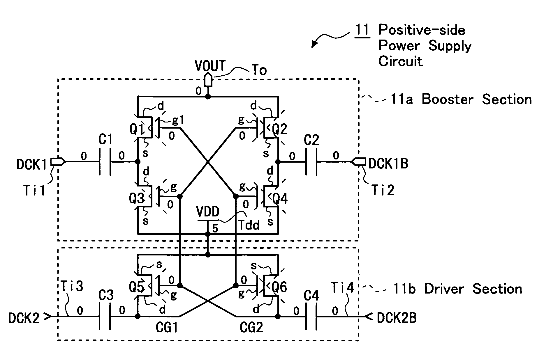
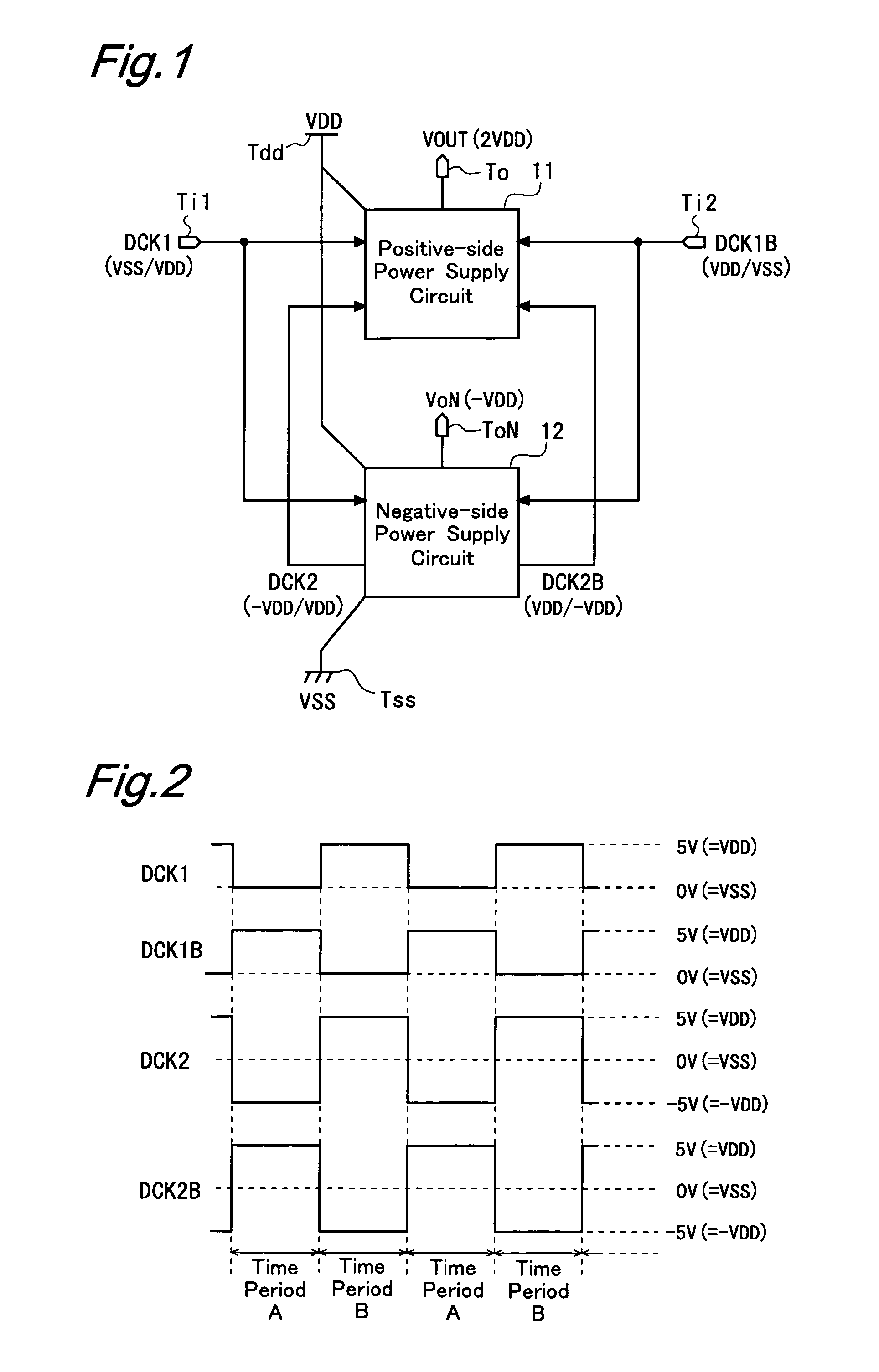
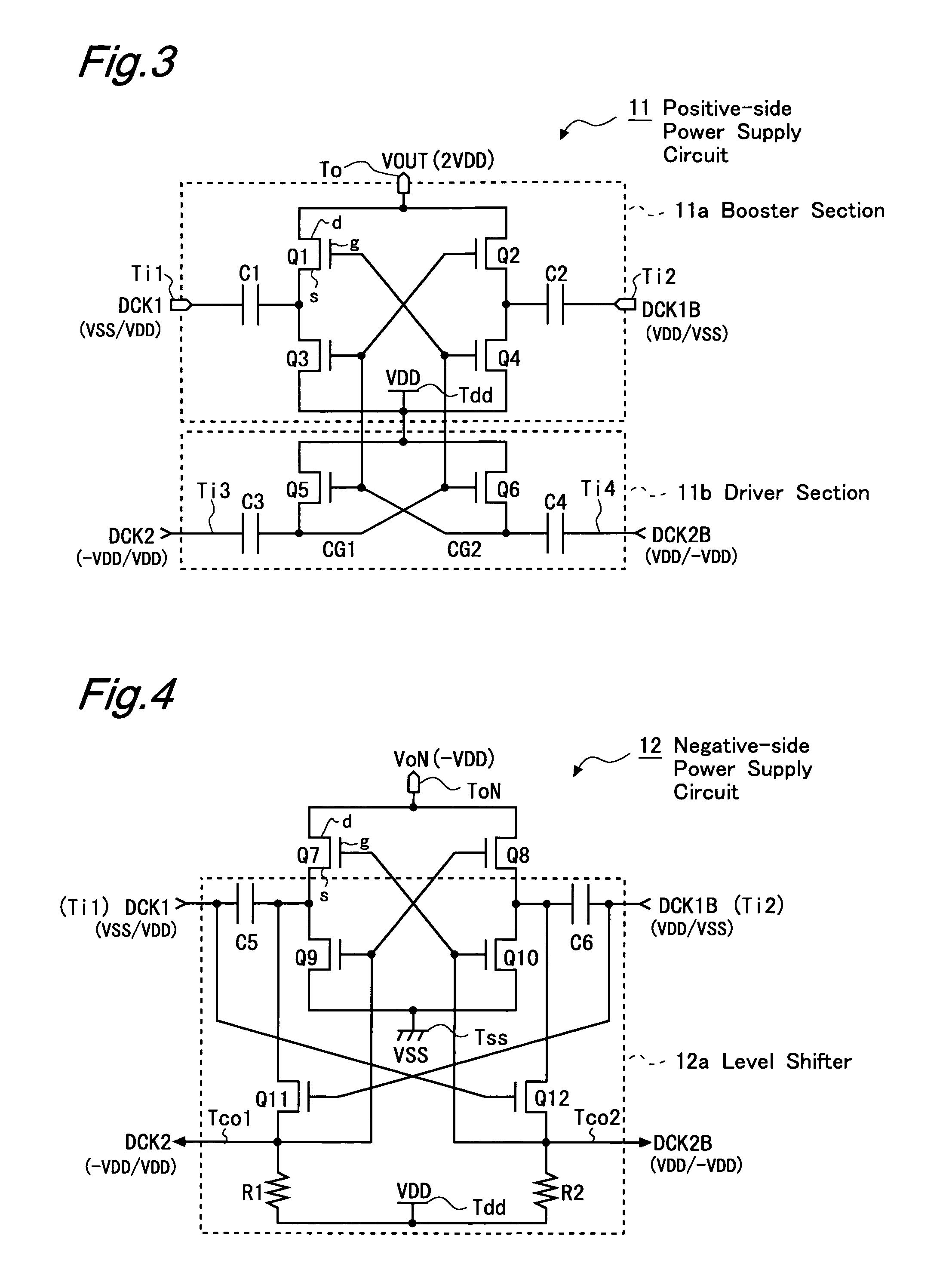
[0139]FIG. 1 is a block diagram which shows a general configuration of a power supply circuit according to an embodiment of the present invention. This power supply circuit includes: a positive-side power supply circuit 11 which functions as a charge-pumping voltage-boosting power supply circuit; and a negative-side power supply circuit 12 which generates a negative supply voltage; and has external terminals including: a first and a second input terminals Ti1 and Ti2 for receiving externally supplied first and second clock signals DCK1 and DCK1B respectively; a power supply terminal Tdd for receiving a positive supply voltage VDD as an input supply voltage from outside; a grounding terminal Tss which is connected to an external grounding line and receives a grounding voltage VSS as a reference potential for the input supply voltage; an output terminal To for outp...


PUM


Abstract

An object of the present invention is to provide a power supply circuit including a charge-pumping booster section which uses switching elements provided only by N-channel transistors yet does not have a problem of voltage drop by threshold value. In a booster section (11a), capacitors (C1) and (C2) have their respective first terminals connected with transistors (Q1, Q3) and (Q2, Q4) respectively. Each transistor has its gate terminal supplied with control signals generated in a driver section (11b). The driver section (11b) includes capacitors (C3, C4) connected with input terminals (Ti3, Ti4) for respective supply of clock signals DCK2, DCK2B each having a voltage alternating between −VDD and VDD (VDD represents an input supply voltage from outside), as level-shifted signals of clock signals DCK1, DCK1B which are supplied to second terminals of the capacitors (C1, C2) respectively. In this arrangement, the driver section 11b generates signals each having a voltage alternating between VDD and 3VDD, as the control signals.

Description

TECHNICAL FIELD[0001]The present invention relates to power supply circuits, and more specifically to a power supply circuit which includes a charge-pumping booster section for boosting a supply voltage, and to a driver monolithic display device which includes such a power supply circuit.BACKGROUND ART[0002]Inductance DC-DC converters for boosting supply voltages are already public. A challenge with this type of DC-DC converters, however, is size reduction since the converter requires inductive elements, and it has long been difficult to implement the converter as a semiconductor circuit. For this reason, when supply voltage boosting is required in portable equipment such as mobile telephone terminals or in integrated circuits, the task is accomplished by charge pump circuits (see Patent Document 1 (JP-A Hei 10-285911 Gazette), for example) which are built with capacitors and switching elements.[0003]In liquid crystal display devices incorporated in mobile telephone terminals for ex...

Claims


Application Information

Patent Timeline
Patent Type & Authority Patents(United States)
IPC IPC(8): G09G5/00
CPCH02M3/073
Inventor TSUJINO, SACHIONISHI, SHUJIMURAKAMI, YUHICHIROHSASAKI, YASUSHIGYOUTEN, SEIJIROU
Owner SHARP KK
Why Eureka
Try Eureka