

Apparatus and method for controlling etch uniformity
- Summary
- Abstract
- Description
- Claims
- Application Information
AI Technical Summary
Benefits of technology
Problems solved by technology
Method used
Image

Examples
Embodiment Construction
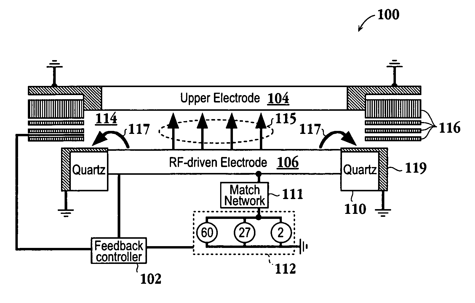
[0016]An invention is described for a method and apparatus, which maintains a bias voltage to ensure uniformity of an etch operation. In one embodiment, adjustments to the bias voltage are achieved through manipulation of the frequency of the radio frequency (RF) power source. It will be obvious, however, to one skilled in the art, that the present invention may be practiced without some or all of these specific details. In other instances, well known process operations have not been described in detail in order not to obscure the present invention.
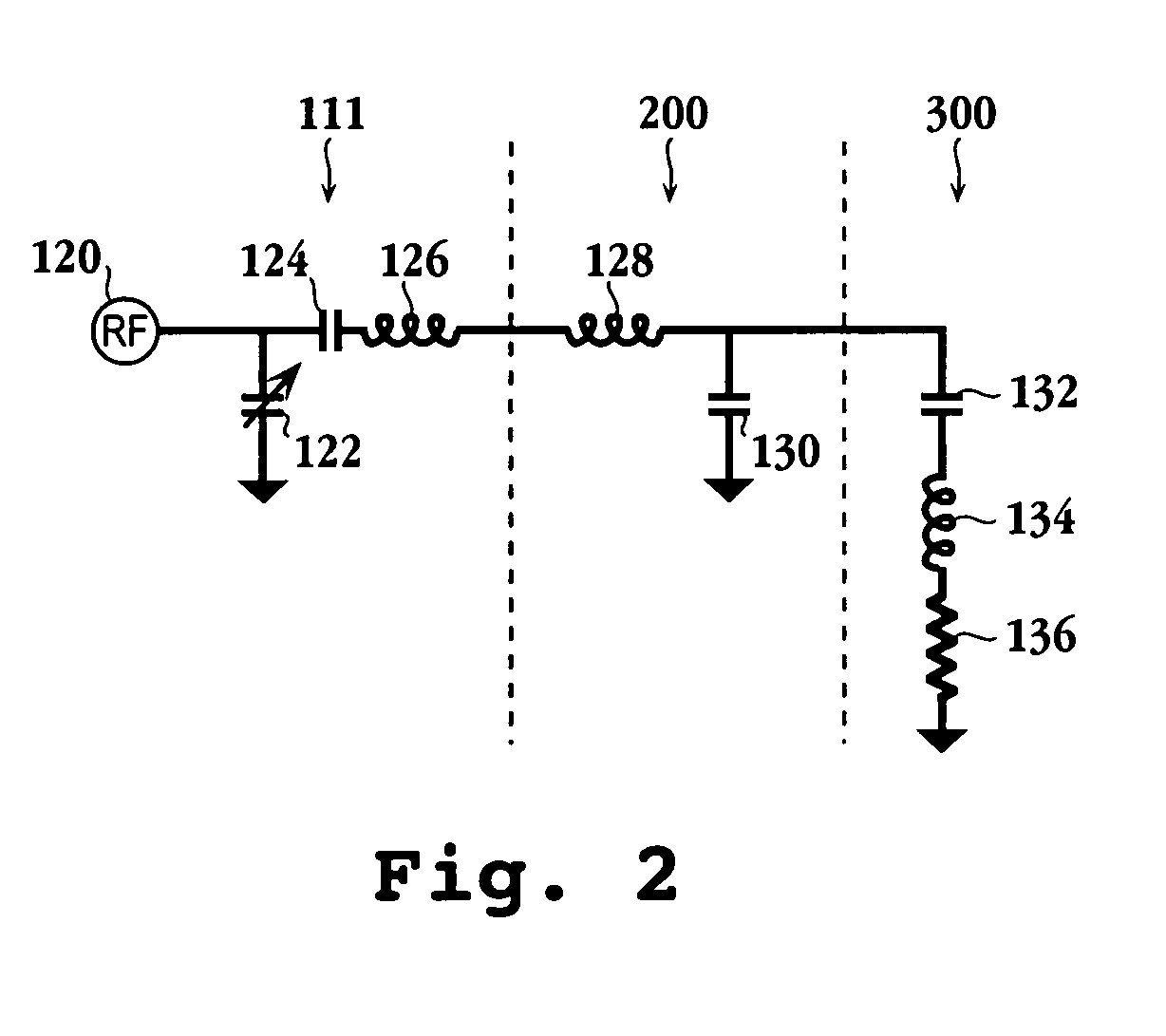
[0017]The embodiments of the present invention provide an apparatus and method for achieving etch uniformity through bias control. Through the embodiments described herein, additional tuning elements are provided so as to enhance etch uniformity control. In one embodiment, the frequency of the RF power supply is tunable, i.e., may be varied, to adjust the etch uniformity. By varying the frequency of the RF power supply, the power delivere...
PUM
| Property | Measurement | Unit |
|---|---|---|
| Fraction | aaaaa | aaaaa |
| Frequency | aaaaa | aaaaa |
| Frequency | aaaaa | aaaaa |
Abstract
Description
Claims
Application Information