Inspection apparatus for lithography

a technology of lithography and inspection apparatus, which is applied in the direction of printing, instruments, material analysis, etc., can solve the problems of not being able to use all azimuthal angles, unable to accurately measure only the intensity of scattered radiation, and risk exacerbating a small error in even a single one of those devices

Active Publication Date: 2014-03-25
ASML NETHERLANDS BV
View PDF7 Cites 30 Cited by
  • Summary
  • Abstract
  • Description
  • Claims
  • Application Information

AI Technical Summary

Problems solved by technology

Although scatterometry is a relatively quick form of analysis of a surface, measuring only the intensity of scattered radiation may not be the most precise of measurements, as it does not take into account the different behavior of radiation that is polarized in different directions.
Furthermore, having several devices in series risks exacerbating a small error in even only a single one of those devices.
Yet furthermore, not all azimuthal angles are useable.
Potentially useful information is therefore lost.

Method used


Image

  • Inspection apparatus for lithography
  • Inspection apparatus for lithography
  • Inspection apparatus for lithography

Examples


Embodiment Construction

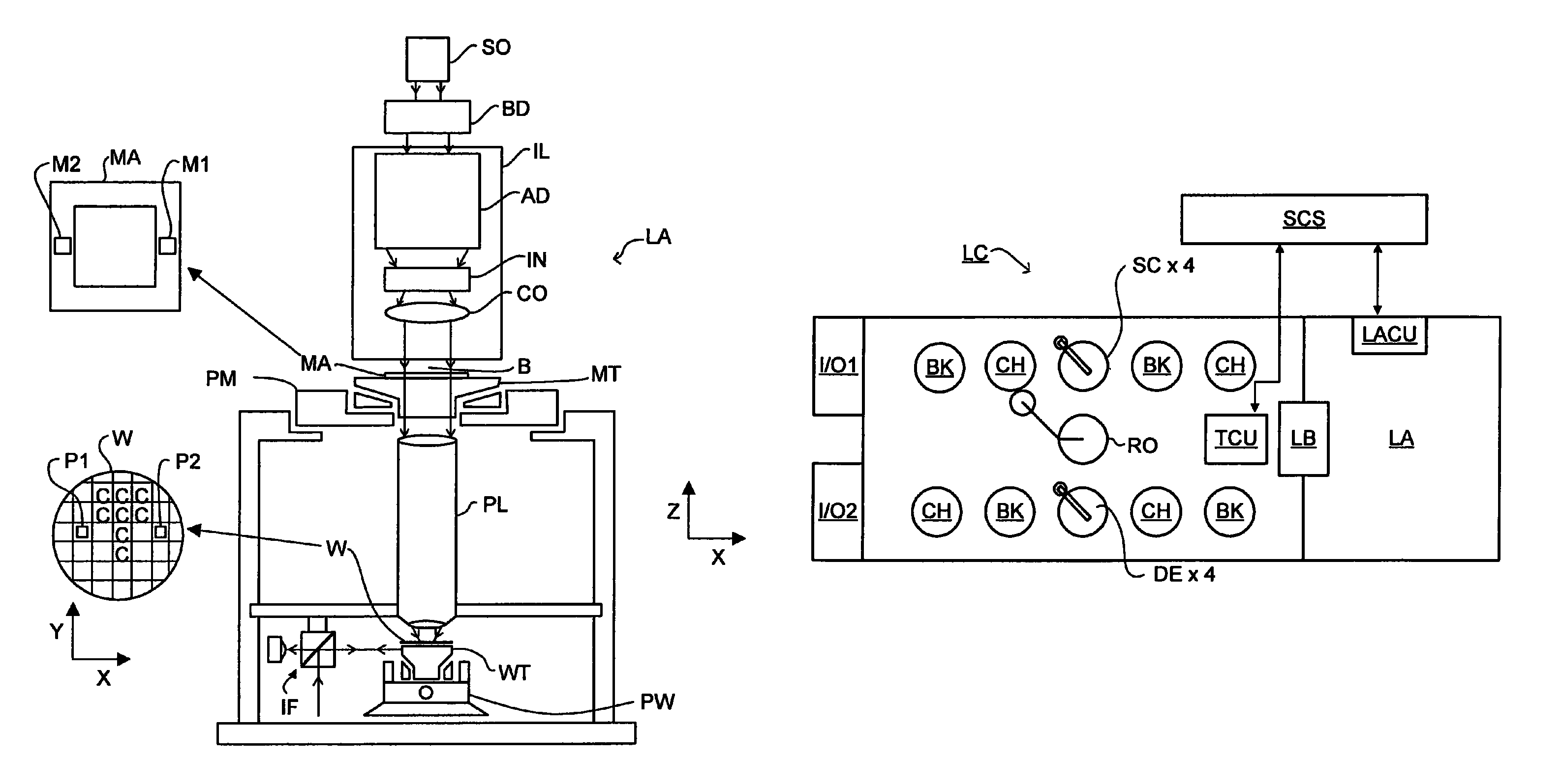
[0020]FIG. 1a schematically depicts a lithographic apparatus. The apparatus includes an illumination system (illuminator) IL configured to condition a radiation beam B (e.g. UV radiation or EUV radiation); a patterning device support or support structure (e.g. a mask table) MT constructed to support a patterning device (e.g. a mask) MA and connected to a first positioner PM configured to accurately position the patterning device in accordance with certain parameters; a substrate table (e.g. a wafer table) WT constructed to hold a substrate (e.g. a resist-coated wafer) W and connected to a second positioner PW configured to accurately position the substrate in accordance with certain parameters; and a projection system (e.g. a refractive projection lens system) PL configured to project a pattern imparted to the radiation beam B by patterning device MA onto a target portion C (e.g. including one or more dies) of the substrate W.

[0021]The illumination system may include various types o...


PUM


Abstract

The measurement of two separately polarized beams (Ix, Iy) upon diffraction from a substrate (W) in order to determine properties of the substrate is disclosed. Circularly or elliptically polarized radiation is passed via a variable phase retarder in order to change the phase of one of two orthogonally polarized radiation beams with respect to the other of the two beams. The phase change is dependent on the wavelength of the polarized beam. The relative phases of the two radiation beams and other features of the beams as measured in a detector gives rise to properties of the substrate surface.

Description

FIELD[0001]The present invention relates to methods of inspection usable, for example, in the manufacture of devices by lithographic techniques and to methods of manufacturing devices using lithographic techniques.BACKGROUND[0002]A lithographic apparatus is a machine that applies a desired pattern onto a substrate, usually onto a target portion of the substrate. A lithographic apparatus can be used, for example, in the manufacture of integrated circuits (ICs). In that instance, a patterning device, which is alternatively referred to as a mask or a reticle, may be used to generate a circuit pattern to be formed on an individual layer of the IC. This pattern can be transferred onto a target portion (e.g. including part of, one, or several dies) on a substrate (e.g. a silicon wafer). Transfer of the pattern is typically via imaging onto a layer of radiation-sensitive material (resist) provided on the substrate. In general, a single substrate will contain a network of adjacent target po...

Claims


Application Information

Patent Timeline
Patent Type & Authority Patents(United States)
IPC IPC(8): G03B27/42
CPCG03F7/70616G01N21/956G01N21/211
Inventor STRAAIJER, ALEXANDER
Owner ASML NETHERLANDS BV
Why Eureka
Try Eureka